SBOS771A December 2016 – January 2019 OPA4277-SP
PRODUCTION DATA.
- 1 Features
- 2 Applications
- 3 Description
- 4 Revision History
- 5 Pin Configuration and Functions
- 6 Specifications
- 7 Detailed Description
- 8 Application and Implementation
- 9 Power Supply Recommendations
- 10Layout
- 11Device and Documentation Support
- 12Mechanical, Packaging, and Orderable Information
Package Options
Mechanical Data (Package|Pins)
Thermal pad, mechanical data (Package|Pins)
Orderable Information
5 Pin Configuration and Functions
HFR Package
14-Pin CFP
Top View
Pin Functions: CFP
| PIN | I/O | DESCRIPTION | |
|---|---|---|---|
| NO. | NAME | ||
| 1 | OUT A | O | Output channel A. |
| 2 | –IN A | I | Inverting input channel A. |
| 3 | +IN A | I | Noninverting input channel A. |
| 4 | V+ | — | Positive (highest) power supply. |
| 5 | +IN B | I | Noninverting input channel B. |
| 6 | –IN B | I | Inverting input channel B. |
| 7 | OUT B | O | Output channel B. |
| 8 | OUT C | O | Output channel C. |
| 9 | –IN C | I | Inverting input channel C. |
| 10 | +IN C | I | Noninverting input channel C. |
| 11 | V– | — | Negative (lowest) power supply. |
| 12 | +IN D | I | Noninverting input channel D. |
| 13 | –IN D | I | Inverting input channel D. |
| 14 | OUT D | O | Output channel D. |
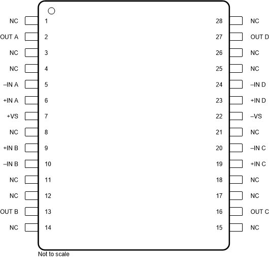
JDJ Package
28-Pin CDIP
Top View

NC - no internal connection
Pin Functions: CDIP
| PIN | I/O | DESCRIPTION | |
|---|---|---|---|
| NO. | NAME | ||
| 1, 3, 4, 8, 11, 12, 14, 15, 17, 18, 21, 25, 26, 28 | NC | — | Not connected. |
| 2 | OUT A | O | Output (channel A). |
| 5 | –IN A | I | Inverting input (channel A). |
| 6 | +IN A | I | Noninverting input (channel A). |
| 7 | +VS | — | Positive (highest) power supply. |
| 9 | +IN B | I | Inverting input (channel B). |
| 10 | –IN B | I | Noninverting input (channel B). |
| 13 | OUT B | O | Output (channel B). |
| 16 | OUT C | O | Output (channel C). |
| 19 | +IN C | I | Inverting input (channel C). |
| 20 | –IN C | I | Noninverting input (channel C). |
| 22 | –VS | — | Negative (lowest) power supply. |
| 23 | +IN D | I | Inverting input (channel D). |
| 24 | –IN D | I | Noninverting input (channel D). |
| 27 | OUT D | O | Output (channel D). |