SCPS178C July 2007 – April 2022 PCA9306-Q1
PRODUCTION DATA
- 1 Features
- 2 Applications
- 3 Description
- 4 Revision History
- 5 Description (continued)
- 6 Pin Configuration and Functions
-
7 Specifications
- 7.1 Absolute Maximum Ratings
- 7.2 ESD Ratings
- 7.3 Recommended Operating Conditions
- 7.4 Thermal Information
- 7.5 Electrical Characteristics
- 7.6 Switching Characteristics: Translating Down, VIH = 3.3 V
- 7.7 Switching Characteristics: Translating Down, VIH = 2.5 V
- 7.8 Switching Characteristics: Translating Up, VIH = 2.3 V
- 7.9 Switching Characteristics: Translating Up, VIH = 1.5 V
- 7.10 Typical Characteristics
- 8 Parameter Measurement Information
-
9 Detailed Description
- 9.1
Overview
- 9.1.1 Definition of threshold voltage
- 9.1.2 Correct Device Set Up
- 9.1.3 Disconnecting a Target from the Main I2C Bus Using the EN Pin
- 9.1.4 Supporting Remote Board Insertion to Backplane with PCA9306-Q1
- 9.1.5 Switch Configuration
- 9.1.6 Controller on Side 1 or Side 2 of Device
- 9.1.7 LDO and PCA9306-Q1 Concerns
- 9.1.8 Current Limiting Resistance on VREF2
- 9.2 Functional Block Diagram
- 9.3 Feature Description
- 9.4 Device Functional Modes
- 9.1
Overview
- 10Application and Implementation
- 11Power Supply Recommendations
- 12Layout
- 13Device and Documentation Support
- 14Mechanical, Packaging, and Orderable Information
Package Options
Mechanical Data (Package|Pins)
- DCU|8
Thermal pad, mechanical data (Package|Pins)
Orderable Information
10.2.2.2 Sizing Pullup Resistor
The pullup resistor value must limit the current through the pass transistor, when it is in the ON state, to about 15 mA. This ensures a pass voltage of 260 mV to 350 mV. If the current through the pass transistor is higher than 15 mA, the pass voltage also is higher in the ON state. To set the current through each pass transistor at 15 mA, the pullup resistor value is calculated as:
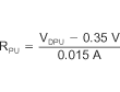
Table 10-2 summarizes resistor values, reference voltages, and currents at 15 mA, 10 mA, and 3 mA. The resistor value shown in the +10% column (or a larger value) must be used to ensure that the pass voltage of the transistor is 350 mV or less. The external driver must be able to sink the total current from the resistors on both sides of the PCA9306-Q1 device at 0.175 V, although the 15 mA applies only to current flowing through the PCA9306-Q1 device.
| PULLUP RESISTOR VALUE (Ω)(1)(2) | ||||||
|---|---|---|---|---|---|---|
| VDPU | 15 mA | 10 mA | 3 mA | |||
| NOMINAL | +10%(3) | NOMINAL | +10%(3) | NOMINAL | +10%(3) | |
| 5 V | 310 | 341 | 465 | 512 | 1550 | 1705 |
| 3.3 V | 197 | 217 | 295 | 325 | 983 | 1082 |
| 2.5 V | 143 | 158 | 215 | 237 | 717 | 788 |
| 1.8 V | 97 | 106 | 145 | 160 | 483 | 532 |
| 1.5 V | 77 | 85 | 115 | 127 | 383 | 422 |
| 1.2 V | 57 | 63 | 85 | 94 | 283 | 312 |