SCPS127F September 2006 – March 2021 PCA9554A
PRODUCTION DATA
- 1 Features
- 2 Description
- 3 Revision History
- 4 Description (Continued)
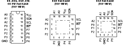
- 5 Pin Configuration And Functions
- 6 Specifications
- 7 Parameter Measurement Information
- 8 Detailed Description
- 9 Application Information Disclaimer
- 10Power Supply Recommendations
- 11Device and Documentation Support
- 12Mechanical, Packaging, and Orderable Information
Package Options
Mechanical Data (Package|Pins)
Thermal pad, mechanical data (Package|Pins)
Orderable Information
2 Description
This 8-bit I/O expander for the two-line bidirectional bus (I2C) is designed for 2.3-V to 5.5-V VCC operation. It provides general-purpose remote I/O expansion for most microcontroller families via the I2C interface [serial clock (SCL), serial data (SDA)].
The PCA9554A consists of one 8-bit Configuration (input or output selection), Input, Output, and Polarity Inversion (active high or active low) registers. At power on, the I/Os are configured as inputs with a weak pullup to VCC. However, the system master can enable the I/Os as either inputs or outputs by writing to the I/O configuration bits. The data for each input or output is kept in the corresponding Input or Output register. The polarity of the Input Port register can be inverted with the Polarity Inversion register. All registers can be read by the system master.
The system master can reset the PCA9554A in the event of a timeout or other improper operation by utilizing the power-on reset feature, which puts the registers in their default state and initializes the I2C/SMBus state machine.
| PART NUMBER | PACKAGE(1) | BODY SIZE (NOM) |
|---|---|---|
| PCA9554A | DB (SSOP) (16) | 6.20 mm × 5.30 mm |
| DBQ (VQFN) (16) | 4.90 mm × 3.90 mm | |
| DGV (TSSOP) (16) | 3.60 mm × 4.40 mm | |
| DW (SOIC) | 10.3 mm x 7.50 mm | |
| PW (TSSOP) | 5.00 mm x 4.40 mm | |
| RGT (VQFN) | 3.00 mm x 3.00 mm | |
| RGV (VQFN) | 4.00 mm x 4.00 mm |