SLES211C February 2008 – July 2015 PCM1681 , PCM1681-Q1
PRODUCTION DATA.
- 1 Features
- 2 Applications
- 3 Description
- 4 Revision History
- 5 Description (continued)
- 6 Pin Configuration and Functions
- 7 Specifications
-
8 Detailed Description
- 8.1 Overview
- 8.2 Functional Block Diagram
- 8.3 Feature Description
- 8.4 Device Functional Modes
- 8.5 Programming
- 8.6
Register Maps
- 8.6.1 Reserved Registers
- 8.6.2
Register Definitions
- 8.6.2.1 ATx[7:0]: Digital Attenuation Level Setting
- 8.6.2.2 MUTx: Soft Mute Control
- 8.6.2.3 DACx: DAC Operation Control
- 8.6.2.4 FLT: Digital Filter Roll-Off Control
- 8.6.2.5 FMT[3:0]: Audio Interface Data Format
- 8.6.2.6 SRST: Reset
- 8.6.2.7 ZREV: Zero-Flag Polarity Select
- 8.6.2.8 DREV: Output Phase Select
- 8.6.2.9 DMF[1:0]: Sampling Frequency Selection for the De-Emphasis Function
- 8.6.2.10 DMC: Digital De-Emphasis All-Channel Function Control
- 8.6.2.11 REV[8:1]: Output Phase Select per Channel
- 8.6.2.12 OVER: Oversampling Rate Control
- 8.6.2.13 FLTx: Digital Filter Roll-Off Control per DATA Group
- 8.6.2.14 DAMS: Digital Attenuation Mode Select
- 8.6.2.15 AZRO[1:0]: Zero-Flag Channel-Combination Select
- 8.6.2.16 ZERO[8:1]: Zero-Detect Status (Read-Only, I2C Interface Only)
- 9 Application and Implementation
- 10Power Supply Recommendations
- 11Layout
- 12Device and Documentation Support
- 13Mechanical, Packaging, and Orderable Information
Package Options
Mechanical Data (Package|Pins)
- PWP|28
Thermal pad, mechanical data (Package|Pins)
- PWP|28
Orderable Information
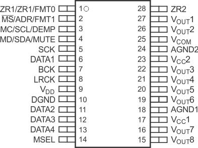
6 Pin Configuration and Functions
PWP Package
28-Pin HTSSOP PowerPAD
Top View

Pin Functions
| PIN | I/O | DESCRIPTION | |
|---|---|---|---|
| NAME | NO. | ||
| AGND1 | 18 | – | Analog ground |
| AGND2 | 24 | – | Analog ground |
| BCK | 7 | I | Shift clock input for serial audio data (1)(2) |
| DATA1 | 6 | I | Serial audio data input for VOUT1 and VOUT2 (1)(2) |
| DATA2 | 11 | I | Serial audio data input for VOUT3 and VOUT4 (1)(2) |
| DATA3 | 12 | I | Serial audio data input for VOUT5 and VOUT6 (1)(2) |
| DATA4 | 13 | I | Serial audio data input for VOUT7 and VOUT8 (1)(2) |
| DGND | 10 | – | Digital ground |
| LRCK | 8 | I | Left and right clock input. The frequency of this clock is equal to the sampling rate, fS. (1)(2) |
| MC/SCL/DEMP | 3 | I | Shift clock input for SPI, serial clock input for I2C, de-emphasis control for H/W (1)(2) |
| MD/SDA/MUTE | 4 | I/O | Serial data input for SPI, serial data input/output for I2C, mute control for H/W (1)(2)(3) |
| MS/ADR/FMT1 | 2 | I | Select input for SPI, address input for I2C, format control input 1 for H/W (1)(2) |
| MSEL | 14 | I | Mode control select, I2C, H/W with narrow mode O/S, H/W with wide mode O/S, SPI select(1)(4) |
| SCK | 5 | I | System clock input. Input frequency is 128, 192, 256, 384, 512, 768, or 1152 fS. (1)(2) |
| VCC1 | 17 | – | Analog power supply, 5-V |
| VCC2 | 23 | – | Analog power supply, 5-V |
| VCOM | 25 | – | Common voltage output. This pin should be bypassed with a 10-μF capacitor to AGND. |
| VDD | 9 | – | Digital power supply, 3.3-V |
| VOUT1 | 27 | O | Voltage output for audio signal corresponding to L-ch on DATA1 |
| VOUT2 | 26 | O | Voltage output for audio signal corresponding to R-ch on DATA1 |
| VOUT3 | 22 | O | Voltage output for audio signal corresponding to L-ch on DATA2 |
| VOUT4 | 21 | O | Voltage output for audio signal corresponding to R-ch on DATA2 |
| VOUT5 | 20 | O | Voltage output for audio signal corresponding to L-ch on DATA3 |
| VOUT6 | 19 | O | Voltage output for audio signal corresponding to R-ch on DATA3 |
| VOUT7 | 16 | O | Voltage output for audio signal corresponding to L-ch on DATA4 |
| VOUT8 | 15 | O | Voltage output for audio signal corresponding to R-ch on DATA4 |
| ZR1/ZR1/FMT0 | 1 | I/O | Zero-flag output 1 for SPI, zero-flag output 1 for I2C, format control input 0 for H/W(1) |
| ZR2 | 28 | O | Zero-flag output 2 |
(1) Schmitt-trigger input.
(2) 5-V tolerant.
(3) Open-drain output in I2C mode.
(4) VDD/2 biased, quad state input.