SLES230A September 2008 – August 2015 PCM2912A
PRODUCTION DATA.
- 1 Features
- 2 Applications
- 3 Description
- 4 Revision History
- 5 Device Comparison Table
- 6 Pin Configuration and Functions
-
7 Specifications
- 7.1 Absolute Maximum Ratings
- 7.2 ESD Ratings
- 7.3 Recommended Operating Conditions
- 7.4 Thermal Information
- 7.5 Electrical Characteristics
- 7.6
Typical Characteristics
- 7.6.1 ADC Digital Decimation Filter Frequency Response
- 7.6.2 ADC Digital High-Pass Filter Frequency Response
- 7.6.3 ADC Analog Antialiasing Filter Frequency Response
- 7.6.4 DAC Digital Interpolation Filter Frequency Response
- 7.6.5 DAC Analog FIR Filter Frequency Response
- 7.6.6 DAC Analog Low-Pass Filter Frequency Response
- 7.6.7 ADC
- 7.6.8 DAC
- 7.6.9 Supply Current
- 8 Parameter Measurement Information
-
9 Detailed Description
- 9.1 Overview
- 9.2 Functional Block Diagram
- 9.3 Feature Description
- 9.4 Device Functional Modes
- 9.5 Programming
- 10Application and Implementation
- 11Power Supply Recommendations
- 12Layout
- 13Device and Documentation Support
- 14Mechanical, Packaging, and Orderable Information
Package Options
Mechanical Data (Package|Pins)
- PJT|32
Thermal pad, mechanical data (Package|Pins)
Orderable Information
9 Detailed Description
9.1 Overview
The PCM2912A is an audio codec with USB connection capability and an analog front-end for headset applications.
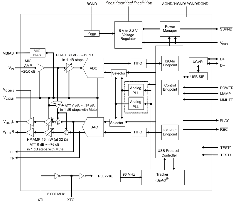
The PCM2912A is a bus-powered device that uses the USB voltage source. The PCM2912A meets the requirements of USB2.0 standard connection. This device has analog and digital inputs and outputs; it has a digital USB interface for input and output data; the analog input is directly routed to the A/D converter and to the analog output. The microphone input has an optional mic amp with fixed +20 dB. The PCM2912A has 2 digital output flags that can be used as LED indicators for Playback and Record. The PCM2912A requires a 12-MHz clock; it can be provided by an external clock or generated by a built-in crystal resonator.
9.2 Functional Block Diagram
9.3 Feature Description
9.3.1 Clock and Reset
The PCM2912A requires a 6-MHz (±500 ppm) clock for USB function and audio function, which can be generated from a built-in crystal oscillator with a 6-MHz crystal resonator. The 6-MHz crystal resonator must be connected to XTI (pin 8) and XTO (pin 7) with one high (1-MΩ) resistor and two small capacitors, whose capacitance depends on the load capacitance of the crystal resonator. An external clock can be supplied through XTI; if an external clock is supplied, XTO must be left open. Because there is no clock disabling signal, using the external clock supply is not recommended. SSPND (pin 29) is unable to use clock disabling.
The PCM2912A has an internal power-on-reset circuit, which works automatically when VBUS (pin 2) exceeds
2.5 V, typical (2.2 V to 2.7 V), and approximately 700 μs is required until the internal reset is released.
9.3.2 DAC
The PCM2912A has a stereo delta-sigma DAC that uses a 64-fS oversampling technique with an 8-fS oversampling digital filter. DAC outputs are provided through the headphone amplifier; VOUTL (pin 18) and VOUTR (pin 22) provide 13 mW at 32 Ω and 0.6 VCCL/VCCR VPP at a 10-kΩ load.
9.3.3 ADC
The PCM2912A has a mono delta-sigma ADC that uses a 64-fS oversampling technique with a 1/64-fS decimation digital filter. The microphone input, VIN (pin 16), is fed to the ADC through a +20-dB microphone amplifier and the PGA, which has +30 dB to –12 dB in 1-dB steps.
9.3.4 Microphone Bias
The PCM2912A has a microphone bias generator, which provides a low-noise, 0.75-VCCA, 2-mA source current output with appropriate output impedance for electret-microphone driving. This output, MBIAS (pin 17), should be bypassed to AGND (pin 13) through an appropriate capacitor to reduce the output noise level.
9.3.5 Microphone Amplifier
The PCM2912A has a low-noise, single-ended, mono microphone amplifier with a mute function that is controlled by MUTE (pin 30). The signal gain is selectable by MAMP (pin 23). The noise level at the input node is 5 μVRMS, and the input impedance is 20 kΩ.
9.3.6 Input PGA
The PCM2912A also has a low-noise input, programmable gain amplifier (PGA) for the microphone amplifier output/ADC input, with a gain range of +30 dB to –12 dB in 1dB/step.
9.3.7 Sidetone Programmable Attenuator
The PCM2912A has a low-noise, sidetone programmable attenuator with a mute function for the sidetone signal path (microphone amplifier output to output PGA input), and a gain range of 0 dB to –76 dB in 1 dB/step.
9.3.8 Output Programmable Attenuator
The PCM2912A has a low-noise output programmable attenuator with a mute function for mixed signal, which affects DAC output signal and sidetone signal. The output PGA gain range is 0 dB to –76 dB in 1 dB/step.
9.3.9 VCOM1 and VCCM2
VCOM2 (pin 12) is provided for the center voltage of the headphone amplifier. VCOM1 (pin 11) is provided for the center voltage of all other analog circuits. Each VCOM pin must be decoupled with an appropriate capacitor. Because the headphone output is disconnected when entering the suspend state, determining the capacitance is important to prevent pop noise, especially for VCOM2 (pin 12). The equivalent resistance of VCOM2 is 500 kΩ, and VCOM1 is 15 kΩ.
9.3.10 Filter Pins
FL (pin 9) and FR (pin 10) are provided to make a low-pass filter (LPF) to decrease the DAC outband noise, as shown in Figure 31. This filter is optional.
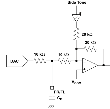 Figure 31. Filter Circuit
9.3.11 Interface Sequence
9.3.11.1 Power-On, Attach, and Play Back Sequence
The PCM2912A is ready for setup when the reset sequence has finished and the USB bus is attached. After a connection has been established, the PCM2912A is ready to accept USB audio data. While waiting for the audio data (that is, in an idle state), the analog output is set to bipolar zero (BPZ).
When receiving the audio data, the PCM2912A stores the first audio packet, which contains 1-ms audio data, into the internal storage buffer. The PCM2912A starts playing the audio data when the subsequent Start of Frame (SOF) packet is detected, as shown in Figure 32.
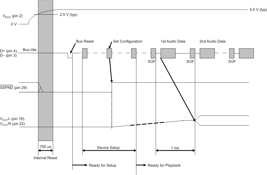 Figure 32. Initial Sequence
9.3.11.2 Play, Stop, and Detach Sequence
When the host finishes or aborts the play back process, the PCM2912A stops playing after last audio data has played, as shown in Figure 33.
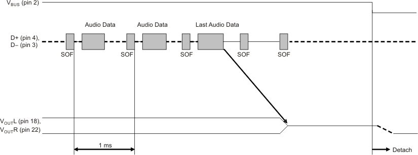 Figure 33. Play, Stop, and Detach
9.3.11.3 Record Sequence
Figure 34 illustrates how the PCM2912A records the audio into the internal memory after receiving the SET_INTERFACE command.
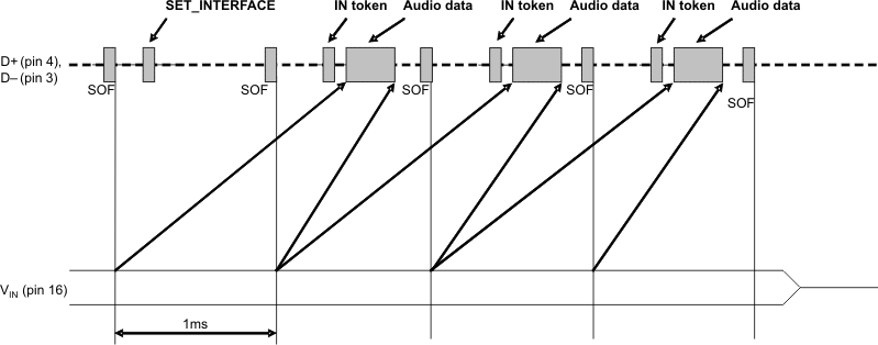 Figure 34. Record Sequence
9.3.11.4 Suspend and Resume Sequence
The PCM2912A enters a suspend state when it sees a constant idle state on the USB bus after approximately
5 ms. When the PCM2912A enters the suspend state, the SSPND flag (pin 29) is asserted. The PCM2912A wakes up immediately after detecting the non-idle state on the USB bus. Figure 35 illustrates these actions.
 Figure 35. Suspend and Resume
9.4 Device Functional Modes
The PCM2912A is a USB-controlled device. The PCM2912A is a codec, with an analog input (that goes to an A/D converter) and analog output (that comes from a D/A converter), alongside the analog path that goes from the microphone input to the headphone output. A wider explanation of these operational modes is shown in Feature Description.
The PCM2912A has hardware controls to turn on and off the integrated microphone preamplifier and the microphone input itself (MAMP and MMUTE, respectively); the microphone preamplifier has +20-dB fixed gain.
9.5 Programming
9.5.1 USB Interface
Control data and audio data are transferred to the PCM2912A via D+ (pin 4) and D– (pin 3). All data transferred to/from the PCM2912A are performed at full speed. Table 1 summarizes the device descriptor. The device descriptor can be modified on request.
Table 1. Device Descriptor
| DEVICE DESCRIPTOR | DESCRIPTION |
|---|---|
| USB revision | 2.0 compliant |
| Device class | 0x00 (device defined in interface level) |
| Device sub class | 0x00 (not specified) |
| Device protocol | 0x00 (not specified) |
| Maximum packet size for endpoint 0 | 8-byte |
| Vendor ID | 0x08BB |
| Product ID | 0x2912 |
| Device release number | 0x0100 (1.00) |
| Number of configurations | 1 |
| Vendor string | String #1 (refer to Table 3) |
| Product string | String #2 (refer to Table 3) |
| Serial number | Not supported |
Table 2 lists the configuration descriptor. The configuration descriptor can be modified on request.
Table 2. Configuration Descriptor
| CONFIGURATION DESCRIPTOR | DESCRIPTION |
|---|---|
| Interface | Three interfaces |
| Power attribute | 0x80 (Bus powered, no remote wakeup) |
| Max power | 0x32 (100 mA at POWER = Low) / 0xFA (500mA at POWER = High) |
Table 3 summarizes the string descriptor. The string descriptor can be modified on request.
Table 3. String Descriptor
| STRING DESCRIPTOR | DESCRIPTION |
|---|---|
| #0 | 0x0409 |
| #1 | Burr-Brown from TI |
| #2 | USB audio CODEC |
9.5.1.1 Device Configuration
Figure 36 illustrates the USB audio function topology. The PCM2912A has three interfaces. Each interface is constructed with some alternative settings.
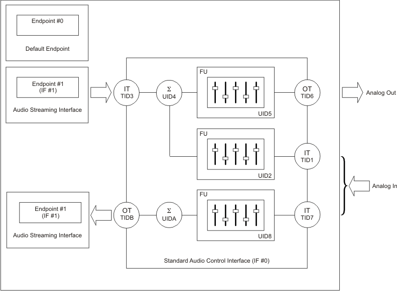 Figure 36. USB Audio Function Topology
9.5.1.2 Interface #0
Interface #0 is the control interface. Alternative setting #0 is the only possible setting for interface #0. Alternative setting #0 describes the standard audio control interface. The audio control interface is constructed with a series of terminal connections. The PCM2912A has the following 10 terminals:
- Input terminal (Terminal ID#1) for audio analog input for sidetone
- Feature unit (Unit ID#2) for sidetone PGA
- Input terminal (Terminal ID#3) for isochronous out stream
- Mixer unit (Unit ID#4) for sidetone mixing
- Feature unit (Unit ID#5) for analog output PGA
- Output terminal (Terminal ID#6) for audio analog output
- Input terminal (Terminal ID#7) for audio analog input
- Feature unit (Unit ID#8) for analog input PGA
- Mixer unit (Unit ID#A) for analog input
- Output terminal (Terminal ID#B) for isochronous in stream
Input terminal #3 is defined as USB stream (terminal type 0x0101). Input terminal #3 can accept two-channel audio streams constructed by the left and right channels. Output terminal #6 is defined as a speaker (terminal type 0x0301). Input terminals #1 and #7 are defined as Microphone (terminal type 0x0201). Physically, these two input terminals are the same input, but logically duplicated. Output terminal B is defined as a USB stream (terminal type 0x0101). Output terminal B is a single-channel audio stream. Mixer unit #4 multiplexes the analog input (sidetone) and the audio data of the digital-to-analog converter (DAC). Mixer unit A is placed in front of output terminal B. Mixer unit A has no impact on recording data. Mixer units #4 and A do not have programming capability.
Feature unit #5 supports the following sound control features for analog outputs:
- Volume control
- Mute control
The built-in volume controller can be manipulated by an audio-class-specific request from 0 dB to –76 dB in steps of 1 dB. An individual (L and R) channel can be set for different values. The built-in mute controller can be manipulated by an audio-class-specific request. Only the master mute control request is acceptable.
Feature unit #2 supports the following sound control features for analog input (sidetone):
- Volume control
- Mute control
The built-in volume controller can be manipulated by an audio-class-specific request from 0 dB to –76 dB in 1-dB steps. Only the master volume control is acceptable. The built-in mute controller can be manipulated by audio-class-specific request. Only the master mute control request is acceptable.
Feature unit #8 supports the following sound control features for analog input (microphone record input):
- Volume control
- Mute control
The built-in analog volume controller can be manipulated by an audio-class-specific request from +30 dB to –12 dB in 1-dB steps. The built-in mute controller can be manipulated by an audio-class-specific request. Only the master mute control request is acceptable.
9.5.1.3 Interface #1
Interface #1 is the audio streaming interface for data output. Table 4 lists the three alternative settings for Interface #1. Alternative setting #0 is the zero bandwidth setting. All other alternative settings are operational settings.
Table 4. Interface #1 Alternative Settings
| ALTERNATIVE SETTING | DATA FORMAT | TRANSFER MODE | SAMPLING RATE (kHz) | ||
|---|---|---|---|---|---|
| 00 | Zero Bandwidth | ||||
| 01 | 16 bit | Stereo | 2s complement (PCM) | Adaptive | 8, 11.025, 16, 22.05, 32, 44.1, 48 |
| 02 | 16 bit | Mono | 2s complement (PCM) | Adaptive | 8, 11.025, 16, 22.05, 32, 44.1, 48 |
9.5.1.4 Interface #2
Interface #2 is the audio streaming interface for data output. Table 5 shows the two alternative settings for Interface #2. Alternative setting #0 is the Zero Band Width setting. Alternative setting #1 is an operational setting.
Table 5. Interface #2 Alternative Settings
| ALTERNATIVE SETTING | DATA FORMAT | TRANSFER MODE | SAMPLING RATE (kHz) | ||
|---|---|---|---|---|---|
| 00 | Zero Bandwidth | ||||
| 01 | 16 bit | Mono | 2s complement (PCM) | Asynchronous | 8, 11.025, 16, 22.05, 32, 44.1, 48 |
9.5.1.5 Endpoints
The PCM2912A has the following three endpoints:
- Control endpoint (EP #0)
- Isochronous out audio data stream endpoint (EP #1)
- Isochronous in audio data stream endpoint (EP #2)
The control endpoint is the default endpoint. The control endpoint controls all functions of the PCM2912A by the standard USB request and USB audio class-specific request from the host. The isochronous out audio data stream endpoint is an audio sink endpoint, which receives the PCM audio data. The isochronous out audio data stream endpoint accepts the asynchronous transfer mode. The isochronous in audio data stream endpoint is an audio source endpoint, which transmits the PCM audio data. The isochronous in audio data stream endpoint uses synchronous transfer mode.
9.5.1.6 Internal Regulator
All required power sources are generated by five internal regulators.
Each regulator generates 3.3 V (typical, without load) from VBUS (pin 2). Each regulator has an output pin and a ground return pin (as described in Table 6); this pair must be decoupled with an appropriate capacitor. Note that this capacitance affects inrush-current limitation. One band-gap reference circuit supplies reference voltage for all regulators. BGND (pin 1) is provided for reference ground of the band-gap reference.
Table 6. Internal Regulator Summary
| SUPPLIED CIRCUIT | OUTPUT | RETURN |
|---|---|---|
| Digital | VDD (pin 5) | DGND (pin 6) |
| Analog | VCCA (pin 15) | AGND (pin 13) |
| Headphone (L-ch) | VCCL (pin 19) | HGND (pin 20) |
| Headphone (R-ch) | VCCR (pin 21) | HGND (pin 20) |
| PLL | VCCP (pin 26) | PGND (pin 25) |