SBVS020C September 2000 – February 2020 REF200
PRODUCTION DATA.
- 1 Features
- 2 Applications
- 3 Description
- 4 Revision History
- 5 Pin Configuration and Functions
- 6 Specifications
- 7 Detailed Description
- 8 Application and Implementation
- 9 Power Supply Recommendations
- 10Layout
- 11Device and Documentation Support
- 12Mechanical, Packaging, and Orderable Information
Package Options
Mechanical Data (Package|Pins)
- D|8
Thermal pad, mechanical data (Package|Pins)
Orderable Information
8.2.2 Detailed Design Procedure
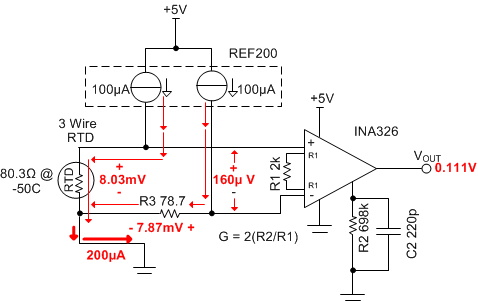
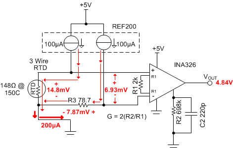
Figure 12 and Figure 13 shows the schematic of the RTD amplifier for minimum and maximum output conditions. This circuit was designed for a –50°C to 150°C RTD temperature range. At –50°C the RTD resistance is 80.3 Ω and the voltage across it is 8.03 mV (VRTD = (100 μA) (80.3 Ω), see Figure 2). Notice that R3 develops a voltage drop that opposes the RTD drop. The drop across R3 is used to shift amplifiers input differential voltage to a minimum level. The output is the differential input multiplied by the gain (Vout = 698 ∙ 160 μV = 0.111 V). At 150°C, the RTD resistance is 148 Ω and the voltage across it is 14. 8 mV (VRTD = (100 μA × 148 Ω ). This produces a differential input of 6.93 mV and an output voltage of 4.84 V (VOUT = 698 ∙ 6.93 mV = 4.84 V , see Figure 13). For more detailed design procedures and results, refer to the reference guide, RTD to Voltage Reference Design Using Instrumentation Amplifier and Current Reference (TIDU969).
 Figure 12. RTD Amplifier with Minimum Output Condition
  Figure 13. RTD Amplifier with Maximum Output Condition