SBVS020C September 2000 – February 2020 REF200
PRODUCTION DATA.
- 1 Features
- 2 Applications
- 3 Description
- 4 Revision History
- 5 Pin Configuration and Functions
- 6 Specifications
- 7 Detailed Description
- 8 Application and Implementation
- 9 Power Supply Recommendations
- 10Layout
- 11Device and Documentation Support
- 12Mechanical, Packaging, and Orderable Information
Package Options
Mechanical Data (Package|Pins)
- D|8
Thermal pad, mechanical data (Package|Pins)
Orderable Information
7.4 Device Functional Modes
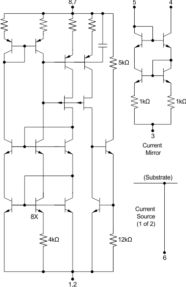
The three circuit sections of the REF200 are electrically isolated from one another, using a dielectrically-isolated fabrication process. A substrate connection is provided (pin 6), which is isolated from all circuitry. This pin should be connected to a defined circuit potential to assure rated DC performance. The preferred connection is to the most negative constant potential in the system. In most analog systems, this would be –VS. For best ac performance, leave pin 6 open and leave unused sections unconnected. Figure 10 shows the simplified circuit diagram of the REF200.
 Figure 10. Simplified Circuit Diagram