SNOSBA3D June 2011 – May 2015 SM74104
PRODUCTION DATA.
- 1 Features
- 2 Typical Applications
- 3 Description
- 4 Revision History
- 5 Pin Configuration and Functions
- 6 Detailed Description
- 7 Application and Implementation
- 8 Power Supply Recommendations
- 9 Layout
- 10Device and Documentation Support
Package Options
Mechanical Data (Package|Pins)
Thermal pad, mechanical data (Package|Pins)
Orderable Information
5 Pin Configuration and Functions
8-Pin SOIC
Package D
Top View

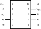
10-Pin WSON
Package DPR
Top View

Pin Functions
| PIN | I/O | DESCRIPTION | ||
|---|---|---|---|---|
| NAME | NO. | |||
| D | DPR | |||
| VDD | 1 | 1 | I | Positive supply voltage input. |
| HB | 2 | 2 | I | Positive connection for high-side bootstrap capacitor. |
| HO | 3 | 3 | O | High-side output to drive the top MOSFET. |
| HS | 4 | 4 | I | Switch node pin. |
| RT | 5 | 7 | I | Delay timer pin. The additional delay of the timer prevents lower and upper MOSFETs from conducting simultaneously, thereby preventing shoot-through. Timer delay is set with a resistor to ground. |
| IN | 6 | 8 | I | PWM control input for LO and HO outputs. |
| VSS | 7 | 9 | - | Ground pin. |
| LO | 8 | 10 | O | Low-side output to drive the bottom MOSFET. |
| N/C | - | 5, 6 | - | No connect. |
| Exposed Pad | - | Exposed Pad | - | The exposed die attach pad (DAP) on the 10-pin WSON package functions as a thermal connection and can be soldered to a copper plane under the device. The DAP nas no direct electrical connection to any of the pins. It can be left floating, but it is recommended to connect this to VSS. |