SNVS903B December 2012 – May 2016 SM74611
PRODUCTION DATA.
- 1 Features
- 2 Applications
- 3 Description
- 4 Revision History
- 5 Pin Configuration and Functions
- 6 Specifications
- 7 Detailed Description
- 8 Application and Implementation
- 9 Power Supply Recommendations
- 10Layout
- 11Device and Documentation Support
- 12Mechanical, Packaging, and Orderable Information
Package Options
Mechanical Data (Package|Pins)
- KTT|3
Thermal pad, mechanical data (Package|Pins)
Orderable Information
7 Detailed Description
7.1 Overview
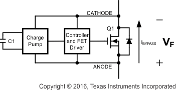
The SM74611 is designed for use as a bypass diode in photovoltaic modules. The SM74611 uses a charge pump to drive an N-channel FET to provide a resistive path for the bypass current to flow.
7.2 Functional Block Diagram

7.3 Feature Description
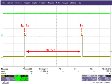
The operational description is described in the following sections. See Figure 4 and Figure 5.
7.3.1 From t0 to t1
When cells in the solar panels are shaded, the FET Q1 is off and the bypass current flows through the body diode of the FET as shown on Figure 4. This current produces a voltage drop (VF) across ANODE and CATHODE terminal of the bypass diode. During this time, the charge pump circuitry is active and charging capacitor C1 to a higher voltage.
7.3.2 At t1
Once the voltage on the capacitor reaches its predetermined voltage level, the charge pump is disabled and the capacitor voltage is used to drive the FET through the FET driver stage.
7.3.3 From t1 to t2
When the FET is active, it provides a low resistive path for the bypass current to flow thus minimizing the power dissipation across ANODE and CATHODE. Because the FET is active, the voltage across the ANODE and CATHODE is too low to operate the charge pump. During this time, the stored charge on C1 is used to supply the controller as well as drive the FET.
7.3.4 At t2
When the voltage on the capacitor C1 reaches its predetermined lower level, the FET driver shuts off the FET. The bypass current will then begin to flow through the body diode of the FET, causing the FET body diode voltage drop of approximately 0.6 V to appear across ANODE and CATHODE. The charge pump circuitry is re-activated and begins charging the capacitor C1. This cycle repeats until the shade on the panel is removed and the string current begins to flow through the PV cells instead of the body diode of the FET.
The key factor to minimizing the power dissipation on the device is to keep the FET on at a high duty cycle. The average forward voltage drop will then be reduced to a much lower voltage than for a Schottky or regular P-N junction diode.
 Figure 5. ANODE to CATHODE Voltage (Ch1) With IBYPASS = 15 A (Ch4) for SM74611 in Junction Box at 85˚C Ambient
7.4 Device Functional Modes
7.4.1 FET Q1 OFF
Initially, the internal FET Q1 is OFF. This is between t0 and t1 as shown in Figure 5. When current begins flowing from ANODE to CATHODE, the FET Q1 body diode conducts with a voltage drop VF.
7.4.2 FET Q1 ON
The FET Q1 is ON between t1 and t2 as shown in Figure 5. During this time, the FET gate is driven and current flows through the FET through a low resistive path.