SCLS263R December 1995 – October 2023 SN54AHCT74 , SN74AHCT74
PRODMIX
- 1
- 1 Features
- 2 Applications
- 3 Description
- 4 Revision History
- 5 Pin Configuration and Functions
- 6 Specifications
- 7 Parameter Measurement Information
- 8 Detailed Description
- 9 Application and Implementation
- 10Device and Documentation Support
- 11Mechanical, Packaging, and Orderable Information
Package Options
Refer to the PDF data sheet for device specific package drawings
Mechanical Data (Package|Pins)
- J|14
- FK|20
- W|14
Thermal pad, mechanical data (Package|Pins)
Orderable Information
3 Description
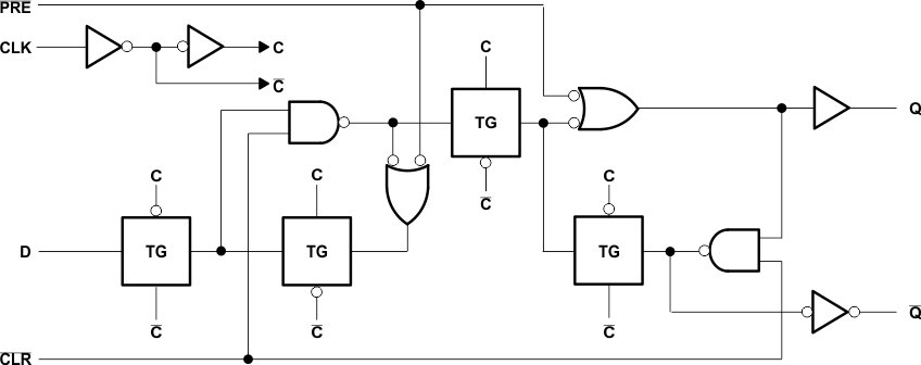
The ’AHCT74 dual positive-edge-triggered devices are D-type flip-flops.
A low level at the preset (PRE) or clear (CLR) inputs sets or resets the outputs, regardless of the levels of the other inputs. When PRE and CLR are inactive (high), data at the data (D) input meeting the setup time requirements is transferred to the outputs on the positive-going edge of the clock pulse. Clock triggering occurs at a voltage level and is not directly related to the rise time of the clock pulse. Following the hold-time interval, data at the D input can be changed without affecting the levels at the outputs.
| PART NUMBER | PACKAGE(1) | PACKAGE SIZE(2) | BODY SIZE (NOM)(3) |
|---|---|---|---|
| SN54AHCT74 | J (CDIP, 14) | 21.3 mm × 7.6 mm | 19.56 mm × 6.67 mm |
| W (CFP, 14) | 13.1 mm × 6.92 mm | 13.1 mm × 6.92 mm | |
| FK (LCCC, 20) | 8.9 mm × 8.9 mm | 8.9 mm × 8.9 mm | |
| SN74AHCT74 | N (PDIP , 14) | 19.3 mm × 8 mm | 19.3 mm × 6.35 mm |
| D (SOIC, 14) | 8.7 mm × 6 mm | 8.7 mm × 3.91 mm | |
| NS (SOP, 14) | 10.3 mm × 7.8 mm | 10.3 mm × 5.3 mm | |
| DB (SSOP, 14) | 6.2 mm × 7.8 mm | 6.2 mm × 5.3 mm | |
| PW (TSSOP, 14) | 5 mm × 6.4 mm | 5 mm × 4.4 mm | |
| DGV (TVSOP, 14) | 3.6 mm × 6.4 mm | 3.6 mm × 4.4 mm | |
| RGY (VQFN, 14) | 3.5 mm × 3.5 mm | 3.50 mm × 3.50 mm | |
| BQA (WQFN, 14) | 3 mm × 2.5 mm | 3.00 mm × 2.50 mm |
 Logic
Diagram, Each Flip-Flop (Positive Logic)