SLLS040I August 1987 – January 2023 SN65ALS176 , SN75ALS176 , SN75ALS176A , SN75ALS176B
PRODUCTION DATA
- 1 Features
- 2 Description
- 3 Revision History
- 4 Pin Configuration and Functions
-
5 Specifications
- 5.1 Absolute Maximum Ratings
- 5.2 Recommended Operating Conditions
- 5.3 Thermal Information
- 5.4 Electrical Characteristics - Driver
- 5.5 Switching Characteristics - Driver
- 5.6 Switching Characteristics - Driver
- 5.7 Symbol Equivalents
- 5.8 Electrical Characteristics - Receiver
- 5.9 Switching Characteristics - Receiver
- 5.10 Switching Characteristics - Receiver
- 5.11 Typical Characteristics
- 6 Parameter Measurement Information
- 7 Detailed Description
- 8 Application and Implementation
- 9 Device and Documentation Support
- 10Mechanical, Packaging, and Orderable Information
Package Options
Refer to the PDF data sheet for device specific package drawings
Mechanical Data (Package|Pins)
- D|8
Thermal pad, mechanical data (Package|Pins)
Orderable Information
2 Description
The SN65ALS176 and SN75ALS176 series differential bus transceivers are designed for bidirectional data communication on multipoint bus transmission lines. The devices are designed for balanced transmission lines and meet TIA/EIA-422-B, TIA/EIA-485-A, and ITU Recommendations V.11 and X.27.
The SN65ALS176 and SN75ALS176 series combine a 3-state, differential line driver and a differential input line receiver, both of which operate from a single 5-V power supply. The driver and receiver have active-high and active-low enables, respectively, that can be connected together externally to function as a direction control. The driver differential outputs and the receiver differential inputs are connected internally to form a differential input/output (I/O) bus port that is designed to offer minimum loading to the bus when the driver is disabled or VCC = 0. This port features wide positive and negative common-mode voltage ranges, making the device suitable for party-line applications.
The SN65ALS176 is characterized for operation from –40°C to 85°C. The SN75ALS176 series is characterized for operation from 0°C to 70°C.
| PART NUMBER | PACKAGE(1) | BODY SIZE (NOM) |
|---|---|---|
| SNx5ALS176 | D (SOIC) | 4.9 mm x 3.91 mm |
| P (PDIP) | 9.81 mm x 6.35 mm | |
| SN75ALS176A | D (SOIC) | 4.9 mm x 3.91 mm |
| P (PDIP) | 9.81 mm x 6.35 mm | |
| SN75ALS176B | D (SOIC) | 4.9 mm x 3.91 mm |
| P (PDIP) | 9.81 mm x 6.35 mm |

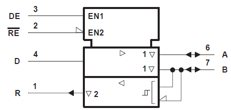
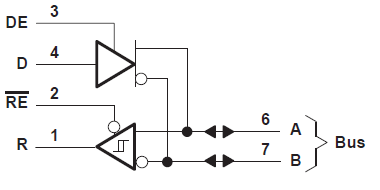
 Logic Diagram (Positive
Logic)