SLLS563I July 2003 – January 2023 SN65HVD1176
PRODUCTION DATA
- 1 Features
- 2 Applications
- 3 Description
- 4 Revision History
- 5 Pin Configuration and Functions
- 6 Specifications
- 7 Detailed Description
- 8 Application and Implementation
- 9 Power Supply Recommendations
- 10Layout
- 11Device and Documentation Support
- 12Mechanical, Packaging, and Orderable Information
Package Options
Mechanical Data (Package|Pins)
- D|8
Thermal pad, mechanical data (Package|Pins)
Orderable Information
Parameter Measurement Information
Note:
Test load capacitance includes probe and jig capacitance (unless otherwise specified).
Signal generator characteristics: rise and fall time < 6 ns, pulse rate 100 kHz, 50% duty cycle, Zo = 50 Ω (unless otherwise specified).
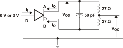 Figure 7-1 Driver Test Circuit, VOD and VOC Without Common-Mode Loading
 Figure 7-2 Driver Test Circuit, VOD With Common-Mode Loading
 Figure 7-3 Driver Switching Test Circuit and Rise/Fall Time Measurement
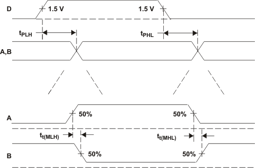 Figure 7-4 Driver Switching Waveforms for Propagation Delay and Output Midpoint Time Measurements
 Figure 7-5 Driver VOC Test Circuit and Waveforms
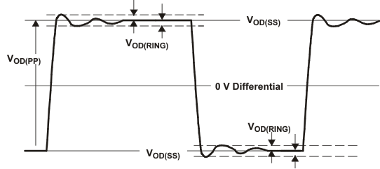
A. VOD(RING) is measured at four points on the output waveform, corresponding to overshoot and undershoot from the VOD(H) and VOD(L) steady state values.
Figure 7-6 VOD(RING) Waveform and Definitions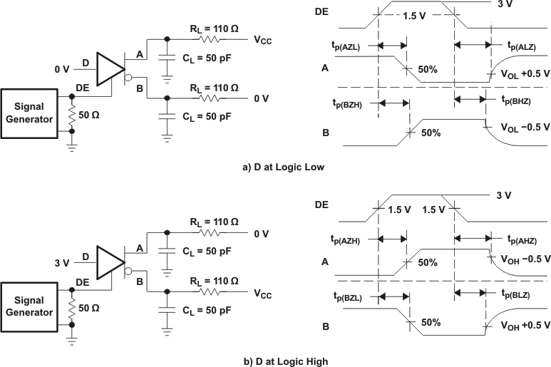 Figure 7-7 Driver Enable/Disable Test
 Figure 7-8 Driver Short-Circuit Test Circuit and Waveforms (Short Circuit applied at Time t = 0)
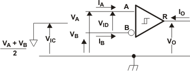 Figure 7-9 Receiver DC Parameter Definitions
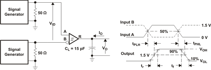 Figure 7-10 Receiver Switching Test Circuit and Waveforms
 Figure 7-11 Receiver Common-Mode Rejection Test Circuit
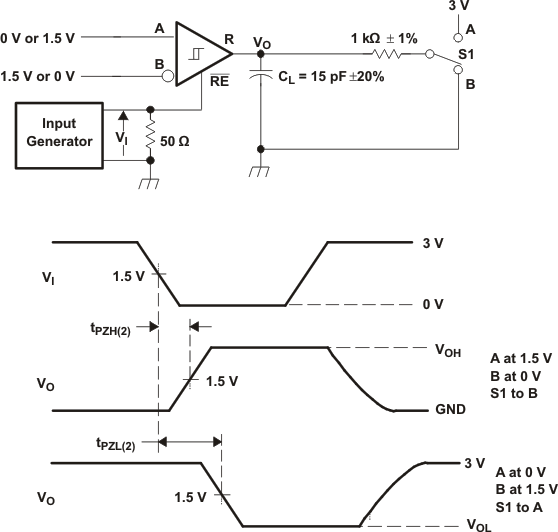 Figure 7-12 Receiver Enable Time From Standby (Driver Disabled)
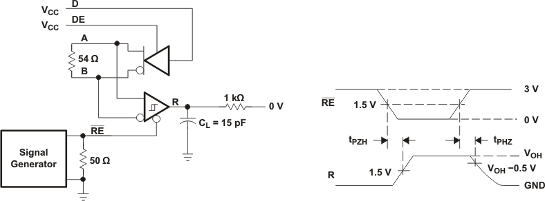 Figure 7-13 Receiver Enable Test Circuit and Waveforms, Data Output High (Driver Active)
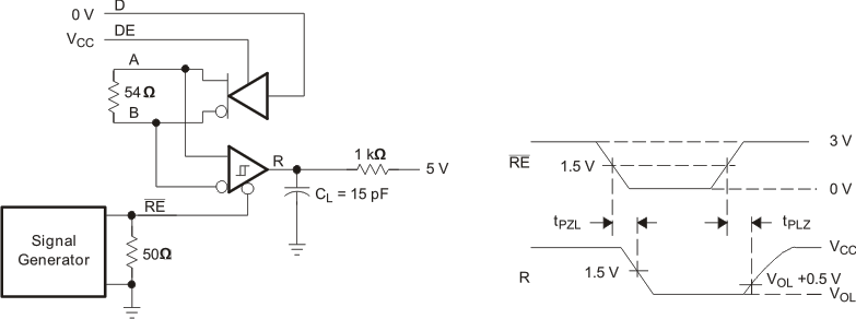 Figure 7-14 Receiver Enable Test Circuit and Waveforms, Data Output Low (Driver Active)
 Figure 7-15 Test Circuit and Waveforms, Transient Overvoltage Test