SLLS563I July 2003 – January 2023 SN65HVD1176
PRODUCTION DATA
- 1 Features
- 2 Applications
- 3 Description
- 4 Revision History
- 5 Pin Configuration and Functions
- 6 Specifications
- 7 Detailed Description
- 8 Application and Implementation
- 9 Power Supply Recommendations
- 10Layout
- 11Device and Documentation Support
- 12Mechanical, Packaging, and Orderable Information
Package Options
Mechanical Data (Package|Pins)
- D|8
Thermal pad, mechanical data (Package|Pins)
Orderable Information
7.4 Device Functional Modes
Table 7-1 Driver Function Table(1)
| INPUT | ENABLE | OUTPUTS | |
|---|---|---|---|
| D | DE | A | B |
| H | H | H | L |
| L | H | L | H |
| X | L | Z | Z |
| X | OPEN | Z | Z |
| OPEN | H | H | L |
(1) H = high level, L = low level, X = don’t care,
Z = high impedance (off)
Z = high impedance (off)
Table 7-2 Receiver Function Table(1)
| DIFFRENTIAL INPUT VID = (VA – VB) | ENABLE RE | OUTPUT R |
|---|---|---|
| VID ≥ –0.02 V | L | H |
| –0.2 V < VID < –0.02 V | L | ? |
| VID ≤ –0.2 V | L | L |
| X | H | Z |
| X | OPEN | Z |
| Open Circuit | L | H |
| Short Circuit | L | H |
| Idle (terminated) bus | L | H |
(1) H = high level, L = low level, X = don’t care,
Z = high impedance (off), ? = indeterminate
Z = high impedance (off), ? = indeterminate
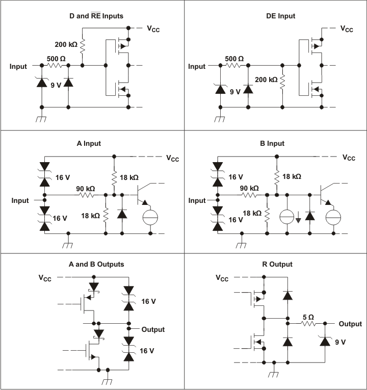
 Figure 7-2 Equivalent Input and Output Schematic Diagrams