SLLS961C July   2009  – June 2022 SN65HVDA195-Q1

PRODUCTION DATA  

  1. Features
  2. Applications
  3. Description
  4. Revision History
  5. Description (continued)
  6. Pin Configuration and Functions
  7. Specifications
    1. 7.1 Absolute Maximum Ratings
    2. 7.2 ESD Ratings
    3. 7.3 Recommended Operating Conditions
    4. 7.4 Thermal Information
    5. 7.5 Electrical Characteristics
    6. 7.6 Typical Characteristics
  8. Parameter Measurement Information
  9. Detailed Description
    1. 9.1 Overview
    2. 9.2 Functional Block Diagram
    3. 9.3 Feature Description
      1. 9.3.1 Local Interconnect Network (LIN) Bus
        1. 9.3.1.1 Transmitter Characteristics
        2. 9.3.1.2 Receiver Characteristics
      2. 9.3.2 Transmit Input (TXD)
      3. 9.3.3 Receive Output (RXD)
        1. 9.3.3.1 RXD Wake-Up Request
      4. 9.3.4 Supply Voltage (VSUP)
      5. 9.3.5 Ground (GND)
      6. 9.3.6 Enable Input (EN)
      7. 9.3.7 NWake Input (NWake)
      8. 9.3.8 Inhibit Output (INH)
    4. 9.4 Device Functional Modes
      1. 9.4.1 Operating Modes
      2. 9.4.2 Normal Mode
      3. 9.4.3 Sleep Mode
      4. 9.4.4 Wake-Up Events
      5. 9.4.5 Standby Mode
  10. 10Application and Implementation
    1. 10.1 Application Information
      1. 10.1.1 Typical Application
        1. 10.1.1.1 Design Requirements
        2. 10.1.1.2 Detailed Design Procedure
        3. 10.1.1.3 Application Curves
      2.      Power Supply Recommendations
      3. 10.1.2 Layout
        1. 10.1.2.1 Layout Guidelines
        2. 10.1.2.2 Layout Example
  11. 11Device and Documentation Support
    1. 11.1 Receiving Notification of Documentation Updates
    2. 11.2 Support Resources
    3. 11.3 Trademarks
    4. 11.4 Electrostatic Discharge Caution
    5. 11.5 Glossary
  12. 12Mechanical, Packaging, and Orderable Information

Package Options

Mechanical Data (Package|Pins)
Thermal pad, mechanical data (Package|Pins)
Orderable Information

Application Curves

Figure 10-2 and Figure 10-3 show the propagation delay from the TXD pin to the LIN pin for both the recessive to dominant and dominant to recessive states under lightly loaded conditions.
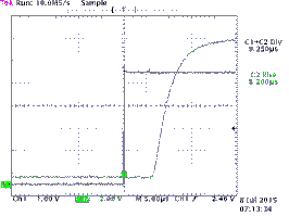
GUID-1DBE0AFF-B4EA-4921-B50B-87D3928DC345-low.gifFigure 10-2 SN65HVDA195-Q1 Dominant to Recessive Prop Delay
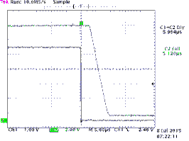
GUID-EC3A5146-7843-4375-8CA7-79EB8BB48BB8-low.gifFigure 10-3 SN65HVDA195-Q1 Recessive to Dominant Prop Delay