SLLS396G SEPTEMBER 1999 – December 2015 SN65LVDS104 , SN65LVDS105
PRODUCTION DATA.
- 1 Features
- 2 Applications
- 3 Description
- 4 Revision History
- 5 Selection Guide to LVDS Repeaters
- 6 Pin Configuration and Functions
-
7 Specifications
- 7.1 Absolute Maximum Ratings
- 7.2 ESD Ratings—JEDEC
- 7.3 ESD Ratings—MIL-STD
- 7.4 Recommended Operating Conditions
- 7.5 Thermal Information
- 7.6 SN65LVDS104 Electrical Characteristics
- 7.7 SN65LVDS105 Electrical Characteristics
- 7.8 SN65LVDS104 Switching Characteristics
- 7.9 SN65LVDS105 Switching Characteristics
- 7.10 Dissipation Ratings
- 7.11 Typical Characteristics
- 8 Parameter Measurement Information
- 9 Detailed Description
-
10Application and Implementation
- 10.1 Application Information
- 10.2
Typical Application
- 10.2.1 Point-to-Point Communications
- 10.2.2 Design Requirements
- 10.2.3
Detailed Design Procedure
- 10.2.3.1 Bypass Capacitance
- 10.2.3.2 Driver Supply Voltage
- 10.2.3.3 Driver Input Voltage
- 10.2.3.4 Driver Output Voltage
- 10.2.3.5 Interconnecting Media
- 10.2.3.6 PCB Transmission Lines
- 10.2.3.7 Termination Resistor
- 10.2.3.8 Receiver Supply Voltage
- 10.2.3.9 Receiver Input Common-Mode Range
- 10.2.3.10 Receiver Input Signal
- 10.2.3.11 Receiver Output Signal
- 10.2.4 Application Curve
- 10.3 Multidrop Communications
- 11Power Supply Recommendations
- 12Layout
- 13Device and Documentation Support
- 14Mechanical, Packaging, and Orderable Information
Package Options
Refer to the PDF data sheet for device specific package drawings
Mechanical Data (Package|Pins)
- PW|16
- D|16
Thermal pad, mechanical data (Package|Pins)
Orderable Information
8 Parameter Measurement Information
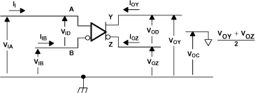
 Figure 13. SN65LVDS104 Voltage and Current Definitions
Table 1. SN65LVDS104 Minimum and Maximum Input Threshold Test Voltages
| APPLIED VOLTAGES |
RESULTING DIFFERENTIAL INPUT VOLTAGE |
RESULTING COMMON-MODE INPUT VOLTAGE |
|
|---|---|---|---|
| VIA | VIB | VID | VIC |
| 1.25 V | 1.15 V | 100 mV | 1.2 V |
| 1.15 V | 1.25 V | –100 mV | 1.2 V |
| 2.4 V | 2.3 V | 100 mV | 2.35 V |
| 2.3 V | 2.4 V | –100 mV | 2.35 V |
| 0.1 V | 0 V | 100 mV | 0.05 V |
| 0 V | 0.1 V | –100 mV | 0.05 V |
| 1.5 V | 0.9 V | 600 mV | 1.2 V |
| 0.9 V | 1.5 V | –600 mV | 1.2 V |
| 2.4 V | 1.8 V | 600 mV | 2.1 V |
| 1.8 V | 2.4 V | –600 mV | 2.1 V |
| 0.6 V | 0 V | 600 mV | 0.3 V |
| 0 V | 0.6 V | –600 mV | 0.3 V |
 Figure 14. SN65LVDS104 VOD Test Circuit

A. All input pulses are supplied by a generator having the following characteristics: tr or tf≤ 1 ns, Pulse Repetition Rate (PRR) = 0.5 Mpps, and pulse width = 500 ± 10 ns.
B. CL includes instrumentation and fixture capacitance within 0.06 m of the device under test. The measurement of VOC(PP) is made on test equipment with a –3 dB bandwidth of at least 300 MHz.
Figure 15. SN65LVDS104 Test Circuit and Definitions for the Driver Common-Mode Output Voltage

A. All input pulses are supplied by a generator having the following characteristics: tr or tf ≤ 1 ns, Pulse Repetition Rate (PRR) = 50 Mpps, and pulse width = 10 ± 0.2 ns.
B. CL includes instrumentation and fixture capacitance within 0.06 m of the device under test.
Figure 16. SN65LVDS104 Test Circuit, Timing, and Voltage Definitions for the Differential Output Signal

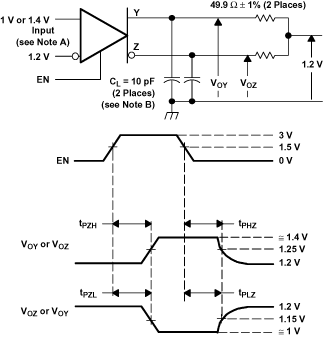
A. All input pulses are supplied by a generator having the following characteristics: tr or tf≤ 1 ns, Pulse Repetition Rate (PRR) = 0.5 Mpps, and pulse width = 500 ± 10 ns.
B. CL includes instrumentation and fixture capacitance within 0.06 m of the device under test.
Figure 17. SN65LVDS104 Enable and Disable Time Circuit and Definitions
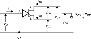
 Figure 18. SN65LVDS105 Voltage and Current Definitions
 Figure 19. SN65LVDS105 VOD Test Circuit

A. All input pulses are supplied by a generator having the following characteristics: tr or tf≤ 1 ns, Pulse Repetition Rate (PRR) = 0.5 Mpps, and pulse width = 500 ± 10 ns.
B. CL includes instrumentation and fixture capacitance within 0.06 m of the device under test. The measurement of VOC(PP) is made on test equipment with a -3 dB bandwidth of at least 300 MHz.
Figure 20. SN65LVDS105 Test Circuit and Definitions for the Driver Common-Mode Output Voltage

A. All input pulses are supplied by a generator having the following characteristics: tr or tf≤ 1 ns, Pulse Repetition Rate (PRR) = 50 Mpps, and pulse width = 10 ± 0.2 ns.
B. CL includes instrumentation and fixture capacitance within 0.06 m of the device under test.
Figure 21. SN65LVDS105 Test Circuit, Timing, and Voltage Definitions for the Differential Output Signal

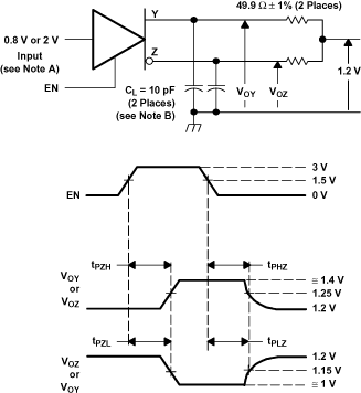
A. All input pulses are supplied by a generator having the following characteristics: tr or tf≤ 1 ns, Pulse Repetition Rate (PRR) = 0.5 Mpps, and pulse width = 500 ± 10 ns.
B. CL includes instrumentation and fixture capacitance within 0.06 m of the device under test.
Figure 22. SN65LVDS105 Enable and Disable Time Circuit and Definitions