SLLS396G SEPTEMBER 1999 – December 2015 SN65LVDS104 , SN65LVDS105
PRODUCTION DATA.
- 1 Features
- 2 Applications
- 3 Description
- 4 Revision History
- 5 Selection Guide to LVDS Repeaters
- 6 Pin Configuration and Functions
-
7 Specifications
- 7.1 Absolute Maximum Ratings
- 7.2 ESD Ratings—JEDEC
- 7.3 ESD Ratings—MIL-STD
- 7.4 Recommended Operating Conditions
- 7.5 Thermal Information
- 7.6 SN65LVDS104 Electrical Characteristics
- 7.7 SN65LVDS105 Electrical Characteristics
- 7.8 SN65LVDS104 Switching Characteristics
- 7.9 SN65LVDS105 Switching Characteristics
- 7.10 Dissipation Ratings
- 7.11 Typical Characteristics
- 8 Parameter Measurement Information
- 9 Detailed Description
-
10Application and Implementation
- 10.1 Application Information
- 10.2
Typical Application
- 10.2.1 Point-to-Point Communications
- 10.2.2 Design Requirements
- 10.2.3
Detailed Design Procedure
- 10.2.3.1 Bypass Capacitance
- 10.2.3.2 Driver Supply Voltage
- 10.2.3.3 Driver Input Voltage
- 10.2.3.4 Driver Output Voltage
- 10.2.3.5 Interconnecting Media
- 10.2.3.6 PCB Transmission Lines
- 10.2.3.7 Termination Resistor
- 10.2.3.8 Receiver Supply Voltage
- 10.2.3.9 Receiver Input Common-Mode Range
- 10.2.3.10 Receiver Input Signal
- 10.2.3.11 Receiver Output Signal
- 10.2.4 Application Curve
- 10.3 Multidrop Communications
- 11Power Supply Recommendations
- 12Layout
- 13Device and Documentation Support
- 14Mechanical, Packaging, and Orderable Information
Package Options
Refer to the PDF data sheet for device specific package drawings
Mechanical Data (Package|Pins)
- PW|16
- D|16
Thermal pad, mechanical data (Package|Pins)
Orderable Information
7 Specifications
7.1 Absolute Maximum Ratings
over operating free-air temperature range (unless otherwise noted) (1)| MIN | MAX | UNIT | ||
|---|---|---|---|---|
| Supply voltage, VCC (2) | –0.5 | 4 | V | |
| Voltage | Enables, A (SN65LVDS105) | –0.5 | 6 | V |
| A, B, Y or Z | –0.5 | 4 | V | |
| Continuous power dissipation | See Dissipation Ratings | |||
| Lead temperature 1.6 mm (1/16 inch) from case for 10 seconds | 260 | °C | ||
| Storage temperature, Tstg | –65 | 150 | °C | |
(1) Stresses beyond those listed under Absolute Maximum Ratings may cause permanent damage to the device. These are stress ratings only, and functional operation of the device at these or any other conditions beyond those indicated under Recommended Operating Conditions is not implied. Exposure to absolute-maximum-rated conditions for extended periods may affect device reliability.
(2) All voltage values, except differential I/O bus voltages, are with respect to network ground terminal.
7.2 ESD Ratings—JEDEC
| VALUE | UNIT | ||||
|---|---|---|---|---|---|
| V(ESD) | Electrostatic discharge | Human body model (HBM), per ANSI/ESDA/JEDEC JS-001(1) | ±12000 | V | |
| Charged-device model (CDM), per JEDEC specification JESD22-C101(2) | ±1500 | ||||
(1) JEDEC document JEP155 states that 500-V HBM allows safe manufacturing with a standard ESD control process.
(2) JEDEC document JEP157 states that 250-V CDM allows safe manufacturing with a standard ESD control process.
7.3 ESD Ratings—MIL-STD
| VALUE | UNIT | |||||
|---|---|---|---|---|---|---|
| V(ESD) | Electrostatic discharge | Tested in accordance with MIL-STD-883C Method 3015.7; A, B, Y, Z, and GND pins | Class 3, A | 16000 | V | |
| Class 3, B | 400 | |||||
7.4 Recommended Operating Conditions
| MIN | NOM | MAX | UNIT | ||
|---|---|---|---|---|---|
| VCC | Supply voltage | 3 | 3.3 | 3.6 | V |
| VIH | High-level input voltage | 2 | V | ||
| VIL | Low-level input voltage | 0.8 | V | ||
| VI or VIC | Voltage at any bus terminal (separately or common-mode) | 0 | VCC–0.8 | ||
| TA | Operating free-air temperature | –40 | 85 | °C | |
7.5 Thermal Information
| THERMAL METRIC(1) | SN65LVDS104, SN65LVDS105 | UNIT | ||
|---|---|---|---|---|
| D (SOIC) | PW (TSSOP) | |||
| 16 PINS | 16 PINS | |||
| RθJA | Junction-to-ambient thermal resistance | 74.4 | 101.6 | °C/W |
| RθJC(top) | Junction-to-case (top) thermal resistance | 35.1 | 29.2 | °C/W |
| RθJB | Junction-to-board thermal resistance | 32 | 47.3 | °C/W |
| ψJT | Junction-to-top characterization parameter | 6 | 1.4 | °C/W |
| ψJB | Junction-to-board characterization parameter | 31.7 | 46.6 | °C/W |
(1) For more information about traditional and new thermal metrics, see the Semiconductor and IC Package Thermal Metrics application report, SPRA953.
7.6 SN65LVDS104 Electrical Characteristics
over recommended operating conditions (unless otherwise noted)| PARAMETER | TEST CONDITIONS | MIN | TYP(1) | MAX | UNIT | |
|---|---|---|---|---|---|---|
| VIT+ | Positive-going differential input voltage threshold | See Figure 13 and Table 1 | 100 | mV | ||
| VIT- | Negative-going differential input voltage threshold | See Figure 13 and Table 1 | –100 | |||
| |VOD| | Differential output voltage magnitude | RL = 100 Ω, VID = ± 100 mV, See Figure 13 and Figure 14 | 247 | 340 | 454 | mV |
| Δ|VOD| | Change in differential output voltage magnitude between logic states | RL = 100 Ω, VID = ± 100 mV, See Figure 13 and Figure 14 | –50 | 50 | mV | |
| VOC(SS) | Steady-state common-mode output voltage | See Figure 15 | 1.125 | 1.375 | V | |
| ΔVOC(SS) | Change in steady-state common-mode output voltage between logic states | See Figure 15 | –50 | 50 | mV | |
| VOC(PP) | Peak-to-peak common-mode output voltage | See Figure 15 | 25 | 150 | mV | |
| ICC | Supply current | Enabled, RL = 100 Ω | 23 | 35 | mA | |
| Disabled | 3 | 8 | ||||
| II | Input current (A or B inputs) | VI = 0 V | –2 | –11 | –20 | µA |
| VI = 2.4 V | –1.2 | –3 | ||||
| II(OFF) | Power-off Input current | VCC = 1.5 V, VI = 2.4 V | 20 | µA | ||
| IIH | High-level input current (enables) | VIH = 2 V | 20 | µA | ||
| IIL | Low-level input current (enables) | VIL = 0.8 V | 10 | µA | ||
| IOS | Short-circuit output current | VOY or VOZ = 0 V | ±10 | mA | ||
| VOD = 0 V | ±10 | |||||
| IOZ | High-impedance output current | VO = 0 V or 2.4 V | ±1 | µA | ||
| IO(OFF) | Power-off output current | VCC = 1.5 V, VO = 2.4 V | ±1 | µA | ||
| CIN | Input capacitance (A or B inputs) | VI = 0.4 sin (4E6πt) + 0.5 V | 3 | pF | ||
| CO | Output capacitance (Y or Z outputs) | VI = 0.4 sin (4E6πt) + 0.5 V, Disabled | 9.4 | pF | ||
(1) All typical values are at 25°C and with a 3.3-V supply.
7.7 SN65LVDS105 Electrical Characteristics
over recommended operating conditions (unless otherwise noted)| PARAMETER | TEST CONDITIONS | MIN | TYP(1) | MAX | UNIT | |
|---|---|---|---|---|---|---|
| |VOD| | Differential output voltage magnitude | RL = 100 Ω, VID = ±100 mV, See Figure 18 and Figure 19 | 247 | 340 | 454 | mV |
| Δ|VOD| | Change in differential output voltage magnitude between logic states | RL = 100 Ω, VID = ±100 mV, See Figure 18 and Figure 19 | –50 | 50 | mV | |
| VOC(SS) | Steady-state common-mode output voltage | See Figure 20 | 1.125 | 1.375 | V | |
| ΔVOC(SS) | Change in steady-state common-mode output voltage between logic states | See Figure 20 | –50 | 50 | mV | |
| VOC(PP) | Peak-to-peak common-mode output voltage | See Figure 20 | 25 | 150 | mV | |
| ICC | Supply current | Enabled, RL = 100 Ω | 23 | 35 | mA | |
| Disabled | 0.7 | 6.4 | ||||
| IIH | High-level input current | VIH = 2 V | 20 | µA | ||
| IIL | Low-level input current | VIL = 0.8 V | 10 | µA | ||
| IOS | Short-circuit output current | VOY or VOZ = 0 V | ±10 | mA | ||
| VOD = 0 V | ±10 | |||||
| IOZ | High-impedance output current | VO = 0 V or 2.4 V | ±1 | µA | ||
| IO(OFF) | Power-off output current | VCC = 1.5 V, VO = 2.4 V | 0.3 | ±1 | µA | |
| CIN | Input capacitance | VI = 0.4 sin (4E6πt) + 0.5 V | 5 | pF | ||
| CO | Output capacitance (Y or Z outputs) | VI = 0.4 sin (4E6πt) + 0.5 V, Disabled | 9.4 | pF | ||
(1) All typical values are at 25°C and with a 3.3-V supply.
7.8 SN65LVDS104 Switching Characteristics
over recommended operating conditions (unless otherwise noted)| PARAMETER | TEST CONDITIONS | MIN | TYP(1) | MAX | UNIT | |
|---|---|---|---|---|---|---|
| tPLH | Propagation delay time, low-to-high-level output | RL = 100 Ω, CL = 10 pF, See Figure 16 | 2.4 | 3.2 | 4.2 | ns |
| tPHL | Propagation delay time, high-to-low-level output | RL = 100 Ω, CL = 10 pF, See Figure 16 | 2.2 | 3.1 | 4.2 | ns |
| tr | Differential output signal rise time | RL = 100 Ω, CL = 10 pF, See Figure 16 | 0.3 | 0.8 | 1.2 | ns |
| tf | Differential output signal fall time | RL = 100 Ω, CL = 10 pF, See Figure 16 | 0.3 | 0.8 | 1.2 | ns |
| tsk(p) | Pulse skew (|tPHL - tPLH|) | RL = 100 Ω, CL = 10 pF, See Figure 16 | 150 | 500 | ps | |
| tsk(o) | Channel-to-channel output skew(2) | RL = 100 Ω, CL = 10 pF, See Figure 16 | 20 | 100 | ps | |
| tsk(pp) | Part-to-part skew(3) | 1.5 | ns | |||
| tPZH | Propagation delay time, high-impedance-to-high-level output | See Figure 17 | 7.2 | 15 | ns | |
| tPZL | Propagation delay time, high-impedance-to-low-level output | See Figure 17 | 8.4 | 15 | ns | |
| tPHZ | Propagation delay time, high-level-to-high-impedance output | See Figure 17 | 3.6 | 15 | ns | |
| tPLZ | Propagation delay time, low-level-to-high-impedance output | See Figure 17 | 6 | 15 | ns | |
(1) All typical values are at 25°C and with a 3.3-V supply.
(2) tsk(o) is the magnitude of the time difference between the tPLH or tPHL of all drivers of a single device with all of their inputs connected together.
(3) tsk(pp) is the magnitude of the difference in propagation delay times between any specified terminals of two devices when both devices operate with the same supply voltages, at the same temperature, and have identical packages and test circuits.
7.9 SN65LVDS105 Switching Characteristics
over recommended operating conditions (unless otherwise noted)| PARAMETER | TEST CONDITIONS | MIN | TYP(1) | MAX | UNIT | |
|---|---|---|---|---|---|---|
| tPLH | Propagation delay time, low-to-high-level output | RL = 100 Ω, CL = 10 pF, See Figure 21 | 1.7 | 2.2 | 3 | ns |
| tPHL | Propagation delay time, high-to-low-level output | RL = 100 Ω, CL = 10 pF, See Figure 21 | 1.4 | 2.3 | 3.5 | ns |
| tr | Differential output signal rise time | RL = 100 Ω, CL = 10 pF, See Figure 21 | 0.3 | 0.8 | 1.2 | ns |
| tf | Differential output signal fall time | RL = 100 Ω, CL = 10 pF, See Figure 21 | 0.3 | 0.8 | 1.2 | ns |
| tsk(p) | Pulse skew (|tPHL - tPLH|) | RL = 100 Ω, CL = 10 pF, See Figure 21 | 150 | 500 | ps | |
| tsk(o) | Channel-to-channel output skew(2) | RL = 100 Ω, CL = 10 pF, See Figure 21 | 20 | 100 | ps | |
| tsk(pp) | Part-to-part skew(3) | 1.5 | ns | |||
| tPZH | Propagation delay time, high-impedance-to-high-level output | See Figure 22 | 7.2 | 15 | ns | |
| tPZL | Propagation delay time, high-impedance-to-low-level output | See Figure 22 | 8.4 | 15 | ns | |
| tPHZ | Propagation delay time, high-level-to-high-impedance output | See Figure 22 | 3.6 | 15 | ns | |
| tPLZ | Propagation delay time, low-level-to-high-impedance output | See Figure 22 | 6 | 15 | ns | |
(1) All typical values are at 25°C and with a 3.3-V supply.
(2) tsk(o) is the magnitude of the time difference between the tPLH or tPHL of all drivers of a single device with all of their inputs connected together.
(3) tsk(pp) is the magnitude of the difference in propagation delay times between any specified terminals of two devices when both devices operate with the same supply voltages, at the same temperature, and have identical packages and test circuits.
7.10 Dissipation Ratings
| PACKAGE | TA≤ 25°C POWER RATING |
OPERATING FACTOR(1)
ABOVE TA = 25°C |
TA = 85°C POWER RATING |
|---|---|---|---|
| D | 950 mW | 7.6 mW/°C | 494 mW |
| PW | 774 mW | 6.2 mW/°C | 402 mW |
(1) This is the inverse of the junction-to-ambient thermal resistance when board-mounted (low-k) and with no air flow.
7.11 Typical Characteristics
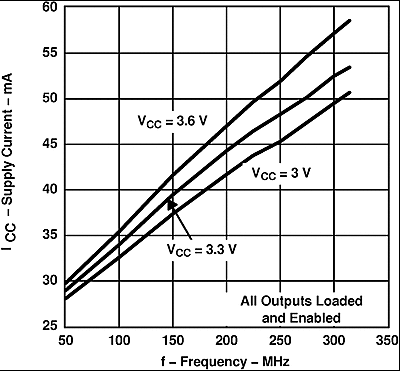 Figure 1. SN65LVDS104 Supply Current vs Frequency
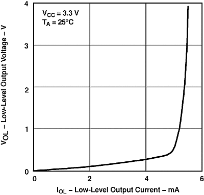 Figure 3. Driver Low-Level Output Voltage vs Low-Level Output Current
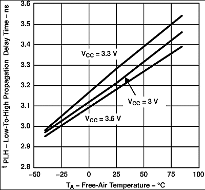 Figure 5. SN65LVDS104 Low-to-High Propagation Delay Time vs Free-Air Temperature
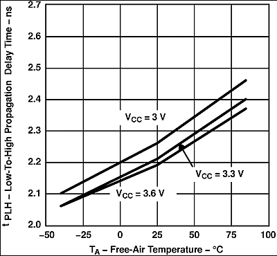 Figure 7. SN65LVDS105 Low-to-High Propagation Delay Time vs Free-Air Temperature
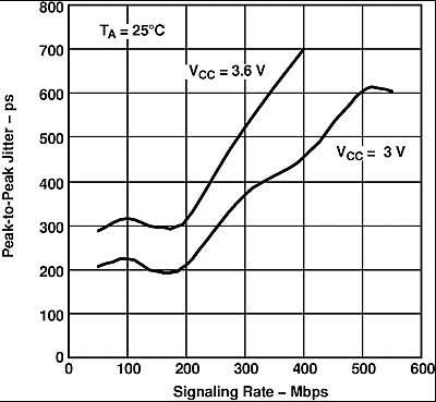
Input: 215 PRBS with peak-to-peak jitter <115 ps at 100 Mbps. Test board adds about 70 ps p-p jitter. All outputs enabled and loaded with differential 100-Ω loads, worst-case output, supply decoupled with 0.1-µF ceramic 0603-style capacitors 1 cm from the device.
Figure 9. SN65LVDS104 P-P Eye-Pattern Jitter vs PRBS Signaling Rate
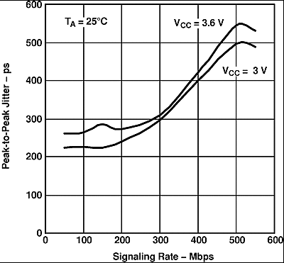
Input: 215 PRBS with peak-to-peak Jitter < 147 ps at 100 Mbps, Test board adds about 43 ps p-p jitter. All outputs enabled and loaded with differential 100-Ω loads, worst-case output, supply decoupled with 0.1-µF and 0.001-µF ceramic 0603-style capacitors 1 cm from the device.
Figure 11. SN65LVDS105 P-P Eye-Pattern Jitter vs PRBS Signaling Rate
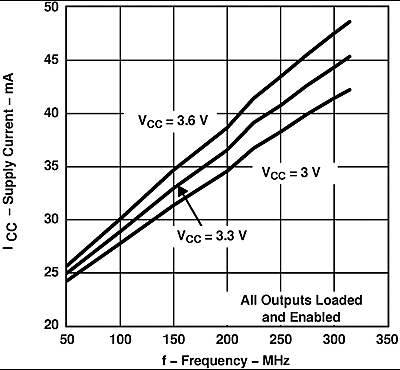 Figure 2. SN65LVDS105 Supply Current vs Frequency
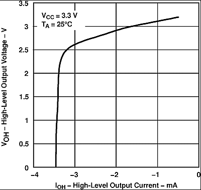 Figure 4. Driver High-Level Output Voltage vs High-Level Output Current
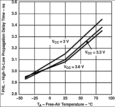 Figure 6. SN65LVDS104 High-to-Low Propagation Delay Time vs Free-Air Temperature
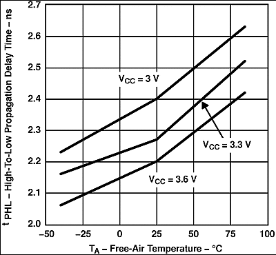 Figure 8. SN65LVDS105 High-to-Low Propagation Delay Time vs Free-Air Temperature
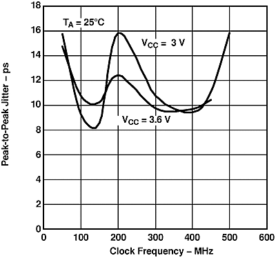
Input: 50% duty cycle square wave with period jitter < 9 ps at 100 MHz. Test board adds about 5 ps p-p jitter. All outputs enabled and loaded with differential 100-Ω loads, worst-case output, supply decoupled with 0.1-µF and 0.001-µF ceramic 0603-style capacitors 1 cm from the device.
Figure 10. SN65LVDS104 P-P Period Jitter vs Clock Frequency
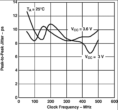
Input: 50% duty cycle square wave with period jitter < 10 ps at 100 MHz. Test board adds about 5 ps p-p jitter. All outputs enabled and loaded with differential 100-Ω loads, worst-case output, supply decoupled with 0.1-µF and 0.001-µF ceramic 0603-style capacitors 1 cm from the device.
Figure 12. SN65LVDS105 P-P Period Jitter vs Clock Frequency