SLLS530C April 2002 – February 2019 SN65LVDT14 , SN65LVDT41
PRODUCTION DATA.
- 1 Features
- 2 Applications
- 3 Description
- 4 Revision History
- 5 Pin Configuration and Functions
-
6 Specifications
- 6.1 Absolute Maximum Ratings
- 6.2 ESD Ratings
- 6.3 Recommended Operating Conditions
- 6.4 Thermal Information
- 6.5 Receiver Electrical Characteristics
- 6.6 Driver Electrical Characteristics
- 6.7 Device Electrical Characteristics
- 6.8 Receiver Switching Characteristics
- 6.9 Driver Switching Characteristics
- 6.10 Typical Characteristics
- 7 Parameter Measurement Information
- 8 Detailed Description
- 9 Application and Implementation
- 10Power Supply Recommendations
- 11Layout
- 12Device and Documentation Support
- 13Mechanical, Packaging, and Orderable Information
Package Options
Refer to the PDF data sheet for device specific package drawings
Mechanical Data (Package|Pins)
- PW|20
Thermal pad, mechanical data (Package|Pins)
- PW|20
Orderable Information
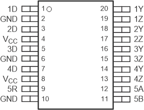
5 Pin Configuration and Functions
SN65LVDT41 PW Package
20-Pin TSSOP
Top View

*marked as LVDT41
SN65LVDT41 Pin Functions
| PIN | I/O | DESCRIPTION | |
|---|---|---|---|
| NAME | NO. | ||
| 1D(1) | 1 | I | LVTTL Driver Input Pin |
| 2D(1) | 3 | ||
| 3D(1) | 5 | ||
| 4D(1) | 7 | ||
| 1Y(1) | 20 | O | Noninverting LVDS Driver Output Pin |
| 2Y(1) | 18 | ||
| 3Y(1) | 16 | ||
| 4Y(1) | 14 | ||
| 1Z(1) | 19 | O | Inverting LVDS Driver Output Pin |
| 2Z(1) | 17 | ||
| 3Z(1) | 15 | ||
| 4Z(1) | 13 | ||
| 5R | 9 | O | LVTTL Receiver Output Pin |
| 5A | 12 | I | Noninverting LVDS Receiver Input Pin |
| 5B | 11 | I | Inverting LVDS Receiver Input Pin |
| VCC | 4, 8 | I | Power Supply Pin, +3.3 V ± 0.3 V |
| GND | 2, 6, 10 | I | Ground Pin |
(1) x = 1, 2, 3, 4 indicating channel number of SN65LVDT41
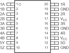
SN65LVDT14 PW Package
20-Pin TSSOP
Top View

*marked as LVDT14
SN65LVDT14 Pin Functions
| PIN | I/O | DESCRIPTION | |
|---|---|---|---|
| NAME | NO. | ||
| 1A(1) | 1 | I | Noninverting LVDS Receiver Input Pin |
| 2A(1) | 3 | ||
| 3A(1) | 5 | ||
| 4A(1) | 7 | ||
| 1B(1) | 2 | I | Inverting LVDS Receiver Input Pin |
| 2B(1) | 4 | ||
| 3B(1) | 6 | ||
| 4B(1) | 8 | ||
| 1R(1) | 20 | O | LVTTL Receiver Output Pin |
| 2R(1) | 18 | ||
| 3R(1) | 16 | ||
| 4R(1) | 14 | ||
| 5Y | 9 | I | Noninverting LVDS Driver Output Pin |
| 5Z | 10 | I | Inverting LVDS Driver Output Pin |
| 5D | 12 | O | LVTTL Driver Input Pin |
| GND | 11, 15, 19 | I | Ground Pin |
| VCC | 13, 17 | I | Power Supply Pin, +3.3 V ± 0.3 V |
(1) x = 1, 2, 3, 4 indicating channel number of SN65LVDT41