SLLS903A December 2009 – March 2024 SN65MLVD048
PRODUCTION DATA
- 1
- 1 Features
- 2 Applications
- 3 Description
- 4 Pin Configuration and Functions
- 5 Specifications
- 6 Parameter Measurement Information
- 7 Device Functional Modes
- 8 Device and Documentation Support
- 9 Revision History
- 10Mechanical, Packaging, and Orderable Information
Package Options
Mechanical Data (Package|Pins)
- RGZ|48
Thermal pad, mechanical data (Package|Pins)
- RGZ|48
Orderable Information
4 Pin Configuration and Functions
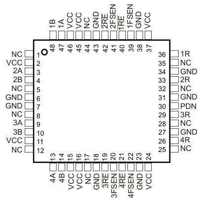
 Figure 4-1 RGZ Package (Top View)
| PIN | I/O(1) | DESCRIPTION | |
|---|---|---|---|
| NAME | NO. | ||
| 1R––4R | 36, 33, 29, 26 | O | Data output from receivers |
| 1A–4A | 47, 3, 9, 13 | I/O | M-LVDS bus non-inverting input/output |
| 1B–4B | 48, 4, 10, 14 | I/O | M-LVDS bus inverting input/output |
| GND | 6, 7, 18, 23, 27, 31, 34, 38, 43 | I | Circuit ground. ALL GND pins must be connected to ground. |
| VCC | 2, 11, 15, 16, 24, 37, 45, 46 | I | Supply voltage. ALL VCC pins must be connected to supply. |
| 1RE– 4RE | 40, 42, 19, 21 | I | Receiver enable, active low, enables individual receivers. When this pin is left floating, internally this pin will be pulled to logic HIGH. |
| 1FSEN–4FSEN | 39, 41, 20, 22 | I | Failsafe enable pin. When this pin is left floating, internally this pin will be pulled to logic HIGH. |
| This pin enables the Type 2 receiver for the respective channel. | |||
| xFSEN = L → Type 1 receiver inputs | |||
| xFSEN = H → Type 2 receiver inputs | |||
| PDN | 30 | Power Down pin. When this pin is left floating, internally this pin will be pulled to logic LOW. | |
| When PDN is HIGH, the device is powered up. | |||
| When PDN is LOW, the device overrides all other control and powers down. All outputs are Hi-Z | |||
| NC | 1, 5, 8, 12, 17, 25, 28, 32, 35 | Not Connected | |
| NC | 44 | Not Connected. Internal TI Test pin. This pin must be left unconnected. | |
| PowerPAD™ | – | Connected to GND | |
(1) Signal Types: I = Input, O = Output, I/O = Input or Output.