SCLS373M May 1996 – April 2024 SN74AHC595
PRODUCTION DATA
- 1
- 1 Features
- 2 Applications
- 3 Description
- 4 Pin Configuration and Functions
-
5 Specifications
- 5.1 Absolute Maximum Ratings
- 5.2 ESD Ratings
- 5.3 Recommended Operating Conditions
- 5.4 Thermal Information
- 5.5 Electrical Characteristics
- 5.6 Timing Requirements: VCC = 3.3 V ± 0.3 V
- 5.7 Timing Requirements: VCC = 5 V ± 0.5 V
- 5.8 Switching Characteristics: VCC = 3.3 V ± 0.3 V
- 5.9 Switching Characteristics: VCC = 5 V ± 0.5 V
- 5.10 Operating Characteristics
- 5.11 Typical Characteristics
- 6 Parameter Measurement Information
- 7 Detailed Description
- 8 Application and Implementation
- 9 Device and Documentation Support
- 10Revision History
- 11Mechanical, Packaging, and Orderable Information
Package Options
Refer to the PDF data sheet for device specific package drawings
Mechanical Data (Package|Pins)
- DB|16
- PW|16
- N|16
- D|16
Thermal pad, mechanical data (Package|Pins)
Orderable Information
3 Description
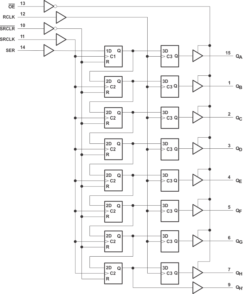
The SN74AHC595 device contains an 8-bit serial-in, parallel-out shift register that feeds an 8-bit D-type storage register. The storage register has parallel 3-state outputs. Separate clocks are provided for both the shift and storage registers. The shift register has a direct overriding clear ( SRCLR) input, a serial (SER) input, and a serial output for cascading. When the output-enable ( OE) input is high, all outputs except QH′ are in the high-impedance state.
Package Information
| PART NUMBER | PACKAGE(1) | PACKAGE SIZE(2) | BODY SIZE(3) |
|---|---|---|---|
| SN74AHC595 | BQB (WQFN, 16) | 3.5mm × 2.5mm | 3.5mm × 2.5mm |
| N (PDIP, 16) | 19.31mm × 9.4mm | 19.31mm × 6.35mm | |
| D (SOIC, 16) | 9.90 mm × 6mm | 9.90mm × 3.90mm | |
| DB (SSOP, 16) | 6.20mm × 7.8mm | 6.20mm × 5.30mm | |
| PW (TSSOP, 16) | 5.00mm × 6.4mm | 5.00 mm × 4.40 mm |
(1) For more information, see Section 11.
(2) The package size (length × width)
is a nominal value and includes pins, where applicable.
(3) The body size (length x width) is
a nominal value and does not include pins.
 Logic Diagram (Positive Logic)