SGDS022B February 2002 – March 2024 SN74AHCT138Q-Q1
PRODUCTION DATA
- 1
- 1 Features
- 2 Description
- 3 Pin Configuration and Functions
- 4 Specifications
- 5 Parameter Measurement Information
- 6 Detailed Description
- 7 Application and Implementation
- 8 Device and Documentation Support
- 9 Revision History
- 10Mechanical, Packaging, and Orderable Information
Package Options
Refer to the PDF data sheet for device specific package drawings
Mechanical Data (Package|Pins)
- PW|16
- D|16
Thermal pad, mechanical data (Package|Pins)
- D|16
Orderable Information
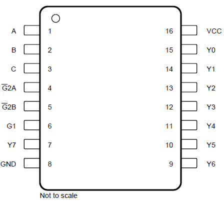
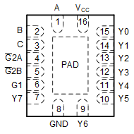
3 Pin Configuration and Functions
 D or PW Package,
16-Pin SOIC or TSSOP
(Top View)
 BQB Package,
16-Pin WBQB
(Top View)
BQB Package,
16-Pin WBQB
(Top View)| PIN | I/O(1) | DESCRIPTION | |
|---|---|---|---|
| NAME | SOIC, TSSOP, WQFN |
||
| A | 1 | I | Select input A (least significant bit) |
| B | 2 | I | Select input B |
| C | 3 | I | Select input C (most significant bit) |
| G2A | 4 | I | Active low enable A |
| G2B | 5 | I | Active low enable B |
| G1 | 6 | I | Active high enable |
| GND | 8 | — | Ground |
| NC | — | — | No internal connection |
| VCC | 16 | — | Supply voltage |
| Y0 | 15 | O | Output 0 (least significant bit) |
| Y1 | 14 | O | Output 1 |
| Y2 | 13 | O | Output 2 |
| Y3 | 12 | O | Output 3 |
| Y4 | 11 | O | Output 4 |
| Y5 | 10 | O | Output 5 |
| Y6 | 9 | O | Output 6 |
| Y7 | 7 | O | Output 7 (most significant bit) |
| Thermal pad(2) | The thermal pad can be connected to GND or left floating. Do not connect to any other signal or supply. | ||
(1) Signal Types: I = Input, O =
Output, I/O = Input or Output, P = Power, G = Ground.
(2) WBQB package only.