SCES598F July 2004 – April 2024 SN74AVCH1T45
PRODUCTION DATA
- 1
- 1 Features
- 2 Applications
- 3 Description
- 4 Description (continued)
- 5 Pin Configuration and Functions
-
6 Specifications
- 6.1 Absolute Maximum Ratings
- 6.2 ESD Ratings
- 6.3 Recommended Operating Conditions
- 6.4 Thermal Information
- 6.5 Electrical Characteristics
- 6.6 Switching Characteristics, VCCA= 1.2V
- 6.7 Switching Characteristics, VCCA= 1.5V ± 0.1V
- 6.8 Switching Characteristics, VCCA= 1.8V ± 0.15V
- 6.9 Switching Characteristics, VCCA= 2.5V ± 0.2V
- 6.10 Switching Characteristics, VCCA= 3.3V ± 0.3V
- 6.11 Operating Characteristics
- 6.12 Typical Characteristics
- 7 Parameter Measurement Information
- 8 Detailed Description
- 9 Application and Implementation
- 10Power Supply Recommendations
- 11Layout
- 12Device and Documentation Support
- 13Revision History
- 14Mechanical, Packaging, and Orderable Information
Package Options
Mechanical Data (Package|Pins)
Thermal pad, mechanical data (Package|Pins)
- DCK|6
Orderable Information
3 Description
The SN74AVCH1T45 is a single-bit noninverting bus transceiver that uses two separate configurable power-supply rails. The A port is designed to track VCCA, which accepts any supply voltage from 1.2V to 3.6V. The B port is designed to track VCCB, which accepts any supply voltage from 1.2V to 3.6V. This feature allows for universal low-voltage, bidirectional translation between any of the 1.2V, 1.5V, 1.8V, 2.5V, and 3.3V voltage nodes.
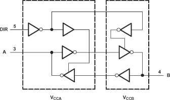
The SN74AVCH1T45 is designed for asynchronous communication between two data buses. The device transmits data from either the A bus to the B bus, or from the B bus to the A bus, depending upon the logic level at the direction-control (DIR) input.
The SN74AVCH1T45 is designed so that the DIR input is referenced to VCCA.
| PART NUMBER | PACKAGE(1) | BODY SIZE (NOM) |
|---|---|---|
| SN74AVCH1T45 | DCK (SC70, 6) | 2.00mm × 1.25mm |
| DBV (SOT-23, 6) | 2.90mm × 1.60mm | |
| YZP (DSBGA, 6) | 1.50mm × 0.90mm |
 Logic Diagram (Positive Logic)