SCAS568N March 1996 – September 2014 SN74LVCH16373A
PRODUCTION DATA.
- 1 Features
- 2 Applications
- 3 Description
- 4 Simplified Schematic
- 5 Revision History
- 6 Pin Configuration and Functions
-
7 Specifications
- 7.1 Absolute Maximum Ratings
- 7.2 Handling Ratings
- 7.3 Recommended Operating Conditions
- 7.4 Thermal Information
- 7.5 Electrical Characteristics
- 7.6 Timing Requirements, -40°C to 85°C
- 7.7 Timing Requirements, -40°C to 125°C
- 7.8 Switching Characteristics, -40°C to 85°C
- 7.9 Switching Characteristics, -40°C to 125°C
- 7.10 Operating Characteristics
- 7.11 Typical Characteristics
- 8 Parameter Measurement Information
- 9 Detailed Description
- 10Application and Implementation
- 11Power Supply Recommendations
- 12Layout
- 13Device and Documentation Support
- 14Mechanical, Packaging, and Orderable Information
Package Options
Refer to the PDF data sheet for device specific package drawings
Mechanical Data (Package|Pins)
- DGG|48
- DL|48
- DGV|48
Thermal pad, mechanical data (Package|Pins)
Orderable Information
9 Detailed Description
9.1 Overview
The SN74LVCH16373A is particularly suitable for implementing buffer registers, I/O ports, bidirectional bus drivers, and working registers. It can be used as two 8-bit latches or one 16-bit latch. When the latch-enable (LE) input is high, the Q outputs follow the data (D) inputs. When LE is taken low, the Q outputs are latched at the levels set up at the D inputs.
A buffered output-enable (OE) input can be used to place the eight outputs in either a normal logic state (high or low logic levels) or the high-impedance state. In the high-impedance state, the outputs neither load nor drive the bus lines significantly. The high-impedance state and increased drive provide the capability to drive bus lines without interface or pull-up components.
OE does not affect internal operations of the latch. Old data can be retained or new data can be entered while the outputs are in the high-impedance state.
Inputs can be driven from either 3.3-V or 5-V devices. This feature allows the use of this device as a translator in a mixed 3.3-V/5-V system environment.
To ensure the high-impedance state during power up or power down, OE should be tied to VCC through a pull-up resistor; the minimum value of the resistor is determined by the current-sinking capability of the driver.
This device is fully specified for partial-power-down applications using Ioff. The Ioff circuitry disables the outputs, preventing damaging current backflow through the device when it is powered down.
Active bus-hold circuitry holds unused or undriven inputs at a valid logic state. Use of pull-up or pull-down resistors with the bus-hold circuitry is not recommended.
9.2 Functional Block Diagram
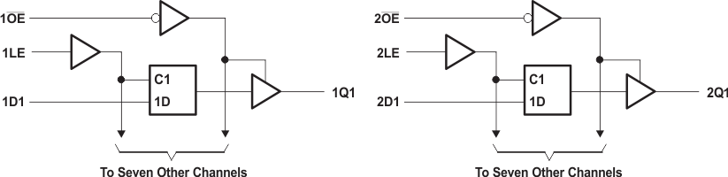 Figure 4. Logic Diagram (Positive Logic)
9.3 Feature Description
- Wide operating voltage range
- Operates from 1.65 V to 3.6 V
- Allows down-voltage translation
- Inputs accept voltages to 5.5 V
- Ioff feature allows voltages on the inputs and outputs when VCC is 0 V
- Bus hold on data inputs eliminates the need for external pull-up or pull-down resistors
9.4 Device Functional Modes
Table 2. Function Table
| INPUTS | OUTPUT Q |
||
|---|---|---|---|
| OE | LE | D | |
| L | H | H | H |
| L | H | L | L |
| L | L | X | Q0 |
| H | X | X | Z |