SLLS159G March 1993 – February 2024 SN65C1167 , SN65C1168 , SN75C1167 , SN75C1168
PRODUCTION DATA
- 1
- 1 Features
- 2 Applications
- 3 Description
- 4 Pin Configuration and Functions
- 5 Specifications
- 6 Parameter Measurement Information
- 7 Detailed Description
- 8 Device and Documentation Support
- 9 Revision History
- 10Mechanical, Packaging, and Orderable Information
Package Options
Refer to the PDF data sheet for device specific package drawings
Mechanical Data (Package|Pins)
- DB|16
- NS|16
- N|16
Thermal pad, mechanical data (Package|Pins)
Orderable Information
3 Description
The SN65C1167, SN75C1167, SN65C1168, and SN75C1168 dual drivers and receivers are integrated circuits designed for balanced transmission lines. The devices meet TIA/EIA-422-B and ITU recommendation V.11.
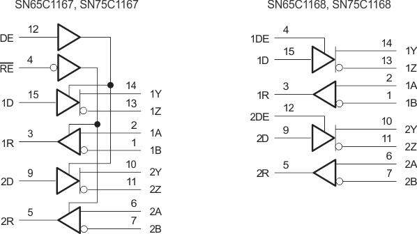
The SN65C1167 and SN75C1167 combine dual 3-state differential line drivers and 3-state differential line receivers, both of which operate from a single 5V power supply. The driver and receiver have active-high and active-low enables, respectively, which can be connected together externally to function as direction control. The SN65C1168 and SN75C1168 drivers have individual active-high enables.
| PART NUMBER | PACKAGE(1) | PACKAGE SIZE(2) |
|---|---|---|
| SN65C1167 | DB (SSOP) | 6.2mm x 5.30mm |
| NS (SOP) | 10.3mm x 5.30mm | |
| SN75C1167 | DB (SSOP) | 6.2mm x 5.30mm |
| N (PDIP) | 19.3mm x 6.35mm | |
| NS (SOP) | 10.3mm x 5.30mm | |
| SN65C1168 | N (PDIP) | 19.3mm x 6.35mm |
| NS (SOP) | 10.3mm x 5.30mm | |
| PW (TSSOP) | 5mm x 4.40mm | |
| SN75C1168 | DB (SSOP) | 6.2mm x 5.30mm |
| N (PDIP) | 19.3mm x 6.35mm | |
| NS (SOP) | 10.3mm x 5.30mm | |
| PW (TSSOP) | 5mm x 4.4mm |
 Logic Diagram (Positive Logic)