SLOS946A May 2016 – December 2016 TAS5722L
PRODUCTION DATA.
- 1 Features
- 2 Applications
- 3 Description
- 4 Revision History
- 5 Pin Configuration and Functions
- 6 Specifications
-
7 Detailed Description
- 7.1 Overview
- 7.2 Functional Block Diagram
- 7.3 Feature Description
- 7.4 Device Functional Modes
- 7.5
Register Maps
- 7.5.1 I2C Register Map Summary
- 7.5.2
Register Maps
- 7.5.2.1 Device Identification Register (0x00)
- 7.5.2.2 Power Control Register (0x01)
- 7.5.2.3 Digital Control Register 1 (0x02)
- 7.5.2.4 Register Name (offset = ) [reset = ] or (address = ) [reset = ]
- 7.5.2.5 Volume Control Register (0x04)
- 7.5.2.6 Analog Control Register (0x06)
- 7.5.2.7 Fault Configuration and Error Status Register (0x08)
- 7.5.2.8 Digital Clipper 2 Register (0x10)
- 7.5.2.9 Digital Clipper 1 Register (0x11)
- 7.5.2.10 Digital Control Register 3 (0x13)
- 7.5.2.11 Analog Control Register 2 (0x14)
- 8 Applications and Implementation
- 9 Power Supply Recommendations
- 10Layout
- 11Device and Documentation Support
- 12Mechanical, Packaging, and Orderable Information
Package Options
Mechanical Data (Package|Pins)
- RSM|32
Thermal pad, mechanical data (Package|Pins)
Orderable Information
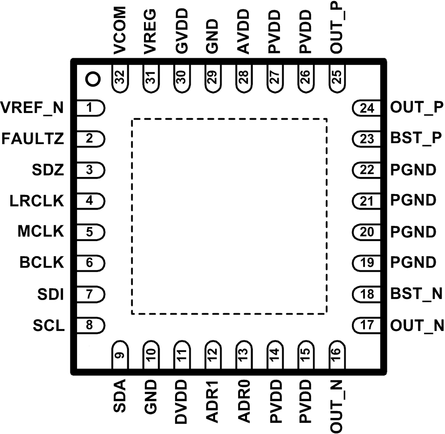
5 Pin Configuration and Functions
RSM PACKAGE
32 PINS
(TOP VIEW)

Pin Functions(2)
| PIN | I/O/P(1) | DESCRIPTION | |
|---|---|---|---|
| NAME | NO. | ||
| ADR1 | 12 | I | I2C address inputs. Each pin can detect a short to DVDD, a short to GND, a 22-kΩ connection to GND and a 22-kΩ connection to DVDD. |
| ADR0 | 13 | I | |
| AVDD | 28 | P | Analog power supply input. Connect directly to PVDD. |
| BCLK | 6 | I | TDM Interface serial bit clock. |
| BST_N | 18 | P | Class-D Amplifier negative bootstrap. Connect a capacitor between BST_N and OUT_N. |
| BST_P | 23 | P | Class-D Amplifier positive bootstrap. Connect a capacitor between BST_P and OUT_P. |
| DVDD | 11 | P | Digital power supply. Connect to 1.8-V supply with external decoupling capacitor. |
| FAULTZ | 2 | O | Open drain active low fault flag. Pull up on PCB with resistor to DVDD. |
| GND | 10 | P | Ground. Connect to PCB ground plane. |
| 29 | |||
| GVDD | 30 | O | Class-D amplifier gate drive regulator output. Connect decoupling cap to PCB ground plane. |
| LRCLK | 4 | I | TDM interface left/right clock. |
| MCLK | 5 | I | Device master clock. |
| PGND | 19 | P | Power ground. Connect to PCB ground plane. |
| 20 | |||
| 21 | |||
| 22 | |||
| PVDD | 14 | P | Class-D amplifier power supply input. Connect to PVDD supply and decouple externally. |
| 15 | |||
| 26 | |||
| 27 | |||
| OUT_N | 16 | O | Class-D amplifier negative output. |
| 17 | |||
| OUT_P | 24 | O | Class-D amplifier positive output. |
| 25 | |||
| SCL | 8 | I | I2C clock Input. Pull up on PCB with a 2.4-kΩ resistor. |
| SDA | 9 | I/O | I2C bi-directional data. Pull up on PCB with a 2.4-kΩ resistor. |
| SDI | 7 | I | TDM interface data input. |
| SDZ | 3 | I | Active low shutdown signal. Assert low to hold device inactive. |
| VCOM | 32 | O | Common mode reference output. Connect decoupling capacitor to the VREF_N pin. |
| VREF_N | 1 | P | Negative reference for analog. Connect to VCOM and VREG capacitor negative pins. |
| VREG | 31 | O | Analog regulator output. Connect decoupling capacitor to the VREF_N pin. |
(1) I = input, O = output, P = power, I/O = bi-directional
(2) Connect exposed thermal pad to PCB ground plane