SLASET9A May   2019  – January 2023 TAS5825P

PRODUCTION DATA  

  1. Features
  2. Applications
  3. Description
  4. Revision History
  5. Device Comparison Table
  6. Pin Configuration and Functions
  7. Specifications
    1. 7.1 Absolute Maximum Ratings
    2. 7.2 ESD Ratings
    3. 7.3 Recommended Operating Conditions
    4. 7.4 Thermal Information
    5. 7.5 Electrical Characteristics
    6. 7.6 Timing Requirements
    7. 7.7 Typical Characteristics
      1. 7.7.1 Bridge Tied Load (BTL) Configuration Curves with Hybrid Modulation
      2. 7.7.2 Parallel Bridge Tied Load (PBTL) Configuration With Hybrid Modulation
      3. 7.7.3 Bridge Tied Load (BTL) Configuration Curves with BD Modulation
      4. 7.7.4 Parallel Bridge Tied Load (PBTL) Configuration With BD Modulation
  8. Parameter Measurement Information
  9. Detailed Description
    1. 9.1 Overview
    2. 9.2 Functional Block Diagram
    3. 9.3 Feature Description
      1. 9.3.1 Power Supplies
      2. 9.3.2 Device Clocking
      3. 9.3.3 Serial Audio Port – Clock Rates
      4. 9.3.4 Clock Halt Auto-Recovery
      5. 9.3.5 Sample Rate on the Fly Change
      6. 9.3.6 Serial Audio Port - Data Formats and Bit Depths
      7. 9.3.7 Digital Audio Processing
      8. 9.3.8 Class-D Audio Amplifier
        1. 9.3.8.1 Speaker Amplifier Gain Select
        2. 9.3.8.2 Class D Loop Bandwidth and Switching Frequency Setting
    4. 9.4 Device Functional Modes
      1. 9.4.1 Software Control
      2. 9.4.2 Speaker Amplifier Operating Modes
        1. 9.4.2.1 BTL Mode
        2. 9.4.2.2 PBTL Mode
      3. 9.4.3 Low EMI Modes
        1. 9.4.3.1 Spread Spectrum
        2. 9.4.3.2 Channel to Channel Phase Shift
        3. 9.4.3.3 Multi-Devices PWM Phase Synchronization
          1. 9.4.3.3.1 Phase Synchronization With I2S Clock In Startup Phase
          2. 9.4.3.3.2 Phase Synchronization With GPIO
      4. 9.4.4 Thermal Foldback
      5. 9.4.5 Device State Control
      6. 9.4.6 Device Modulation
        1. 9.4.6.1 BD Modulation
        2. 9.4.6.2 1SPW Modulation
        3. 9.4.6.3 Hybrid Modulation
    5. 9.5 Programming and Control
      1. 9.5.1 I2 C Serial Communication Bus
      2. 9.5.2 I2 C Peripheral Address
        1. 9.5.2.1 Random Write
        2. 9.5.2.2 Sequential Write
        3. 9.5.2.3 Random Read
        4. 9.5.2.4 Sequential Read
        5. 9.5.2.5 DSP Memory Book, Page and BQ update
        6. 9.5.2.6 Checksum
          1. 9.5.2.6.1 Cyclic Redundancy Check (CRC) Checksum
          2. 9.5.2.6.2 Exclusive or (XOR) Checksum
      3. 9.5.3 Control via Software
        1. 9.5.3.1 Startup Procedures
        2. 9.5.3.2 Shutdown Procedures
        3. 9.5.3.3 Protection and Monitoring
          1. 9.5.3.3.1 Overcurrent Limit (Cycle-By-Cycle)
          2. 9.5.3.3.2 Overcurrent Shutdown (OCSD)
          3. 9.5.3.3.3 DC Detect
    6. 9.6 Register Maps
      1. 9.6.1 CONTROL PORT Registers
  10. 10Application and Implementation
    1. 10.1 Application Information
      1. 10.1.1 Bootstrap Capacitors
      2. 10.1.2 Inductor Selections
      3. 10.1.3 Power Supply Decoupling
      4. 10.1.4 Output EMI Filtering
    2. 10.2 Typical Applications
      1. 10.2.1 2.0 (Stereo BTL) System
      2. 10.2.2 79
      3. 10.2.3 Design Requirements
      4. 10.2.4 Detailed Design procedures
        1. 10.2.4.1 Step One: Hardware Integration
        2. 10.2.4.2 Step Two: Hardware Integration
        3. 10.2.4.3 Step Three: Software Integration
      5. 10.2.5 Application Curves
      6. 10.2.6 MONO (PBTL) Systems
      7. 10.2.7 Application Curves
    3. 10.3 Power Supply Recommendations
      1. 10.3.1 DVDD Supply
      2. 10.3.2 PVDD Supply
    4. 10.4 Layout
      1. 10.4.1 Layout Guidelines
        1. 10.4.1.1 General Guidelines for Audio Amplifiers
        2. 10.4.1.2 Importance of PVDD Bypass Capacitor Placement on PVDD Network
        3. 10.4.1.3 Optimizing Thermal Performance
          1. 10.4.1.3.1 Device, Copper, and Component Layout
          2. 10.4.1.3.2 Stencil Pattern
            1. 10.4.1.3.2.1 PCB footprint and Via Arrangement
            2. 10.4.1.3.2.2 Solder Stencil
      2. 10.4.2 Layout Example
  11. 11Device and Documentation Support
    1. 11.1 Device Support
      1. 11.1.1 Device Nomenclature
      2. 11.1.2 Development Support
    2. 11.2 Receiving Notification of Documentation Updates
    3. 11.3 Support Resources
    4. 11.4 Trademarks
    5. 11.5 Electrostatic Discharge Caution
    6. 11.6 Glossary
  12. 12Mechanical, Packaging, and Orderable Information

Package Options

Mechanical Data (Package|Pins)
Thermal pad, mechanical data (Package|Pins)
Orderable Information

Inductor Selections

TI requires that the peak current is smaller than the OCP (Over current protection) value which is 7.5 A, there are 3 cases which cause high peak current flow through inductor.

  1. During power up (idle state, no audio input), the duty cycle increases from 0 to θ.
    Equation 1. GUID-249A55FA-1347-429F-A16E-BF02BB8AAD49-low.gif
    Note:

    θ=0.5 (BD Modulation), 0.14 (1SPW Modulation), 0.14 (Hybrid Modulation)
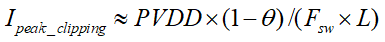
    Table 10-1 Peak Current During Power Up
    PVDDL (µH)C (µF)Fsw (kHz)Ipeak_power_up
    244.70.683846.07A
    244.70.687683.25A
    24100.683843A
    24100.687681.55A
    124.70.683843.32A
    12100.683841.55A
  2. During music playing, some audio burst signal (high frequency) with very hard PVDD clipping causes PWM duty cycle increase dramatically. This is the worst case and rarely happens.
    Equation 2. GUID-E11B7C12-0C20-443A-8A02-2A8C43D8D8B4-low.gif
  3. Peak current due to Max output power. Ignore the ripple current flow through capacitor here.
    Equation 3. GUID-DBF931BB-4A55-4268-8B36-57FE37C38F13-low.gif

Same PVDD and switching frequency, larger inductance means smaller idle current for lower power dissipation. It's suggested that inductor saturation current ISAT, is larger than the amplifier peak current during power-up and play audio.

Equation 4. GUID-007C12C0-0719-492A-99C5-8E140BF0DD47-low.gif

In addition, the effective inductance at the peak current is required to be at least 80% of the inductance value in Table 10-2 to meet data sheet specifications.

Table 10-2 Inductor Requirements
PVDD (V)Switching Frequency (kHz)Minimum Inductance (L) (µH)
≤ 123844.7
> 1238410

For higher switching frequencies (Fsw), select the inductors with minimum inductance to be 384 kHz / Fsw × L.