SNAS854 February   2023 TDC1000-Q1

PRODUCTION DATA  

  1. Features
  2. Applications
  3. Description
  4. Revision History
  5. Pin Configuration and Functions
  6. Specifications
    1. 6.1 Absolute Maximum Ratings
    2. 6.2 ESD Ratings
    3. 6.3 Recommended Operating Conditions
    4. 6.4 Thermal Information (1)
    5. 6.5 Electrical Characteristics
    6. 6.6 Timing Requirements
    7. 6.7 Switching Characteristics
    8. 6.8 Typical Characteristics
  7. Parameter Measurement Information
  8. Detailed Description
    1. 8.1 Overview
    2. 8.2 Functional Block Diagram
    3. 8.3 Feature Description
      1. 8.3.1 Transmitter Signal Path
      2. 8.3.2 Receiver Signal Path
      3. 8.3.3 Low Noise Amplifier (LNA)
      4. 8.3.4 Programmable Gain Amplifier (PGA)
      5. 8.3.5 Receiver Filters
      6. 8.3.6 Comparators for STOP Pulse Generation
        1. 8.3.6.1 Threshold Detector and DAC
        2. 8.3.6.2 Zero-Cross Detect Comparator
        3. 8.3.6.3 Event Manager
      7. 8.3.7 Common-Mode Buffer (VCOM)
      8. 8.3.8 Temperature Sensor
        1. 8.3.8.1 Temperature Measurement With Multiple RTDs
        2. 8.3.8.2 Temperature Measurement With a Single RTD
    4. 8.4 Device Functional Modes
      1. 8.4.1 Time-of-Flight Measurement Mode
        1. 8.4.1.1 Mode 0
        2. 8.4.1.2 Mode 1
        3. 8.4.1.3 Mode 2
      2. 8.4.2 State Machine
      3. 8.4.3 TRANSMIT Operation
        1. 8.4.3.1 Transmission Pulse Count
        2. 8.4.3.2 TX 180° Pulse Shift
        3. 8.4.3.3 Transmitter Damping
      4. 8.4.4 RECEIVE Operation
        1. 8.4.4.1 Single Echo Receive Mode
        2. 8.4.4.2 Multiple Echo Receive Mode
      5. 8.4.5 Timing
        1. 8.4.5.1 Timing Control and Frequency Scaling (CLKIN)
        2. 8.4.5.2 TX/RX Measurement Sequencing and Timing
      6. 8.4.6 Time-of-Flight (TOF) Control
        1. 8.4.6.1 Short TOF Measurement
        2. 8.4.6.2 Standard TOF Measurement
        3. 8.4.6.3 Standard TOF Measurement With Power Blanking
        4. 8.4.6.4 Common-Mode Reference Settling Time
        5. 8.4.6.5 TOF Measurement Interval
      7. 8.4.7 Averaging and Channel Selection
      8. 8.4.8 Error Reporting
    5. 8.5 Programming
      1. 8.5.1 Serial Peripheral Interface (SPI)
        1. 8.5.1.1 Chip Select Bar (CSB)
        2. 8.5.1.2 Serial Clock (SCLK)
        3. 8.5.1.3 Serial Data Input (SDI)
        4. 8.5.1.4 Serial Data Output (SDO)
    6. 8.6 Register Maps
  9. Application and Implementation
    1. 9.1 Application Information
    2. 9.2 Typical Applications
      1. 9.2.1 Level and Fluid Identification Measurements
        1. 9.2.1.1 Design Requirements
        2. 9.2.1.2 Detailed Design Procedure
          1. 9.2.1.2.1 Level Measurements
          2. 9.2.1.2.2 Fluid Identification
        3. 9.2.1.3 Application Curves
      2. 9.2.2 Water Flow Metering
        1. 9.2.2.1 Design Requirements
        2. 9.2.2.2 Detailed Design Procedure
          1. 9.2.2.2.1 Regulations and Accuracy
          2. 9.2.2.2.2 Transit-Time in Ultrasonic Flow Meters
          3. 9.2.2.2.3 ΔTOF Accuracy Requirement Calculation
          4. 9.2.2.2.4 Operation
        3. 9.2.2.3 Application Curves
    3. 9.3 Power Supply Recommendations
    4. 9.4 Layout
      1. 9.4.1 Layout Guidelines
      2. 9.4.2 Layout Example
  10. 10Device and Documentation Support
    1. 10.1 Device Support
      1. 10.1.1 Development Support
    2. 10.2 Receiving Notification of Documentation Updates
    3. 10.3 Support Resources
    4. 10.4 Trademarks
    5. 10.5 Electrostatic Discharge Caution
    6. 10.6 Glossary
  11. 11Mechanical, Packaging, and Orderable Information

Package Options

Mechanical Data (Package|Pins)
Thermal pad, mechanical data (Package|Pins)
Orderable Information

Temperature Measurement With Multiple RTDs

The temperature measurement mode is selected by setting the MEAS_MODE bit in the CONFIG_2 register to 1. A temperature measurement is started by sending a trigger pulse. After the temperature measurement is complete, the TDC1000-Q1 returns to SLEEP mode. To return to TOF measurement mode, reset the MEAS_MODE bit to 0.

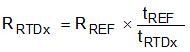
The temperature sensor measurement can be performed without the need of an external ADC. The temperature sensor block operates by converting the resistance of a reference, RREF, and up to two RTDs into a series of START and STOP pulses. The interval between the pulses is proportional to the measured resistance, and therefore, the temperature. As shown in #SNAS6487888, the TDC1000-Q1 performs three measurements per trigger event and generates the corresponding pulses on the START and STOP pins.

GUID-9E7EAC51-652C-4CB2-8D62-DEB6734CC304-low.gifFigure 8-11 Temperature Measurement Output Timing

The resistance of RTD1 and RTD2 can be calculated from the time intervals in #SNAS6487888 as follows:

Equation 3. GUID-0B2FE9BF-C0B9-4566-B571-4C3C309D279A-low.gif

With a 1-kΩ reference resistor, the tREF interval is approximately 200 μs. The following intervals, tRTD1 and tRTD2, will depend on the resistance of the RTDs. The time delay between measurements, td1 and td2, can be approximated as follows:

Equation 4. td1 = (51 × TTEMP) + ( tRTD1 × 0.55 )
Equation 5. td2 = (51 × TTEMP) + ( tRTD2 × 0.55 )

For example, two PT1000 sensors at 0°C will have an approximate resistance of 1 kΩ; the same as the reference resistor in this example. Given an external 8-MHz clock and the default temperature clock divide-by-8 from the TEMP_CLK_DIV bit, the overall measurement time between the START pulse and the last STOP pulse is approximately 922 µs.