SBOS758E May   2016  – May 2021 THS6212

PRODUCTION DATA  

  1. Features
  2. Applications
  3. Description
  4. Revision History
  5. Pin Configuration and Functions
  6. Specifications
    1. 6.1 Absolute Maximum Ratings
    2. 6.2 ESD Ratings
    3. 6.3 Recommended Operating Conditions
    4. 6.4 Thermal Information
    5. 6.5 Electrical Characteristics: VS = 12 V
    6. 6.6 Electrical Characteristics: VS = 28 V
    7. 6.7 Timing Requirements
    8. 6.8 Typical Characteristics: VS = 12 V
    9. 6.9 Typical Characteristics: VS = 28 V
  7. Detailed Description
    1. 7.1 Overview
    2. 7.2 Functional Block Diagram
    3. 7.3 Feature Description
      1. 7.3.1 Output Voltage and Current Drive
      2. 7.3.2 Driving Capacitive Loads
      3. 7.3.3 Distortion Performance
      4. 7.3.4 Differential Noise Performance
      5. 7.3.5 DC Accuracy and Offset Control
    4. 7.4 Device Functional Modes
  8. Application and Implementation
    1. 8.1 Application Information
    2. 8.2 Typical Applications
      1. 8.2.1 Wideband Current-Feedback Operation
        1. 8.2.1.1 Design Requirements
        2. 8.2.1.2 Detailed Design Procedure
        3. 8.2.1.3 Application Curves
      2. 8.2.2 Dual-Supply Downstream Driver
        1. 8.2.2.1 Design Requirements
        2. 8.2.2.2 Detailed Design Procedure
          1. 8.2.2.2.1 Line Driver Headroom Requirements
          2. 8.2.2.2.2 Computing Total Driver Power for Line-Driving Applications
    3. 8.3 What To Do and What Not to Do
      1. 8.3.1 What To Do
      2. 8.3.2 What Not to Do
  9. Power Supply Recommendations
  10. 10Layout
    1. 10.1 Layout Guidelines
    2. 10.2 Layout Example
  11. 11Device and Documentation Support
    1. 11.1 Documentation Support
      1. 11.1.1 Related Documentation
    2. 11.2 Receiving Notification of Documentation Updates
    3. 11.3 Support Resources
    4. 11.4 Trademarks
    5. 11.5 Electrostatic Discharge Caution
    6. 11.6 Glossary
  12. 12Mechanical, Packaging, and Orderable Information

Package Options

Mechanical Data (Package|Pins)
Thermal pad, mechanical data (Package|Pins)
Orderable Information

Differential Noise Performance

The THS6212 is designed to be used as a differential driver in high-performance applications. Therefore, analyzing the noise in such a configuration is important. Figure 7-3 shows the op amp noise model for the differential configuration.

GUID-34BE3E25-58C8-4D13-9962-2DFC02232AAD-low.gifFigure 7-3 Differential Op Amp Noise Analysis Model

As a reminder, the differential gain is expressed in Equation 1:

Equation 1. GUID-A44EB829-DCFF-4CAF-B68A-746F8A96B1CB-low.gif

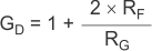
The output noise can be expressed as shown in Equation 2:

Equation 2. GUID-7A3C9431-8773-4250-BEA8-D6947EE606DE-low.gif

Dividing this expression by the differential noise gain [GD = (1 + 2RF / RG)] gives the equivalent input-referred spot noise voltage at the noninverting input, as shown in Equation 3.

Equation 3. GUID-03019F89-C65E-4A96-B43E-A860B404CE72-low.gif

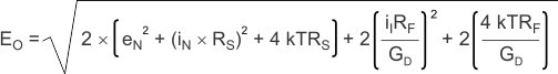
Evaluating these equations for the THS6212 circuit and component values of Figure 8-1 with RS = 50 Ω, gives a total output spot noise voltage of 53.3 nV/√ Hz and a total equivalent input spot noise voltage of 6.5 nV/√ Hz.

In order to minimize the output noise as a result of the noninverting input bias current noise, keeping the noninverting source impedance as low as possible is recommended.