SBOS758E May   2016  – May 2021 THS6212

PRODUCTION DATA  

  1. Features
  2. Applications
  3. Description
  4. Revision History
  5. Pin Configuration and Functions
  6. Specifications
    1. 6.1 Absolute Maximum Ratings
    2. 6.2 ESD Ratings
    3. 6.3 Recommended Operating Conditions
    4. 6.4 Thermal Information
    5. 6.5 Electrical Characteristics: VS = 12 V
    6. 6.6 Electrical Characteristics: VS = 28 V
    7. 6.7 Timing Requirements
    8. 6.8 Typical Characteristics: VS = 12 V
    9. 6.9 Typical Characteristics: VS = 28 V
  7. Detailed Description
    1. 7.1 Overview
    2. 7.2 Functional Block Diagram
    3. 7.3 Feature Description
      1. 7.3.1 Output Voltage and Current Drive
      2. 7.3.2 Driving Capacitive Loads
      3. 7.3.3 Distortion Performance
      4. 7.3.4 Differential Noise Performance
      5. 7.3.5 DC Accuracy and Offset Control
    4. 7.4 Device Functional Modes
  8. Application and Implementation
    1. 8.1 Application Information
    2. 8.2 Typical Applications
      1. 8.2.1 Wideband Current-Feedback Operation
        1. 8.2.1.1 Design Requirements
        2. 8.2.1.2 Detailed Design Procedure
        3. 8.2.1.3 Application Curves
      2. 8.2.2 Dual-Supply Downstream Driver
        1. 8.2.2.1 Design Requirements
        2. 8.2.2.2 Detailed Design Procedure
          1. 8.2.2.2.1 Line Driver Headroom Requirements
          2. 8.2.2.2.2 Computing Total Driver Power for Line-Driving Applications
    3. 8.3 What To Do and What Not to Do
      1. 8.3.1 What To Do
      2. 8.3.2 What Not to Do
  9. Power Supply Recommendations
  10. 10Layout
    1. 10.1 Layout Guidelines
    2. 10.2 Layout Example
  11. 11Device and Documentation Support
    1. 11.1 Documentation Support
      1. 11.1.1 Related Documentation
    2. 11.2 Receiving Notification of Documentation Updates
    3. 11.3 Support Resources
    4. 11.4 Trademarks
    5. 11.5 Electrostatic Discharge Caution
    6. 11.6 Glossary
  12. 12Mechanical, Packaging, and Orderable Information

Package Options

Mechanical Data (Package|Pins)
Thermal pad, mechanical data (Package|Pins)
Orderable Information

DC Accuracy and Offset Control

A current-feedback op amp such as the THS6212 provides exceptional bandwidth in high gains, giving fast pulse settling but only moderate dc accuracy. The Electrical Characteristics tables describe an input offset voltage that is comparable to high-speed, voltage-feedback amplifiers; however, the two input bias currents are somewhat higher and are unmatched. Although bias current cancellation techniques are very effective with most voltage-feedback op amps, these techniques do not generally reduce the output dc offset for wideband current-feedback op amps. Because the two input bias currents are unrelated in both magnitude and polarity, matching the input source impedance to reduce error contribution to the output is ineffective. Evaluating the configuration of Figure 8-1, using a typical condition at 25°C input offset voltage and the two input bias currents, gives a typical output offset range equal to Equation 4:
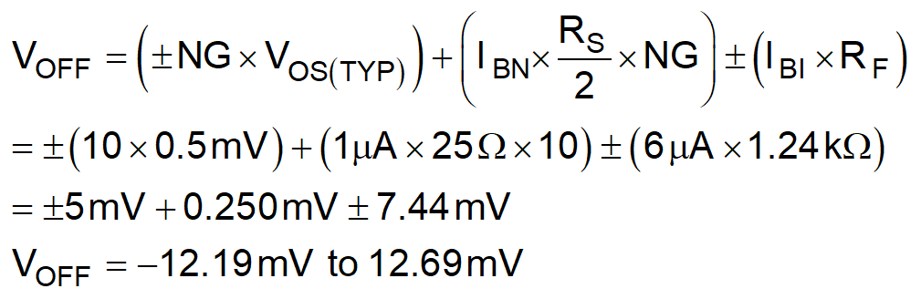
Equation 4. GUID-20210423-CA0I-L0SZ-XSSV-QHPLZM9D9QKX-low.png

where

  • NG = noninverting signal gain