SBOS974D August 2019 – April 2021 THS6222
PRODUCTION DATA
- 1 Features
- 2 Applications
- 3 Description
- 4 Revision History
- 5 Pin Configuration and Functions
- 6 Specifications
- 7 Detailed Description
- 8 Application and Implementation
- 9 Power Supply Recommendations
- 10Layout
- 11Device and Documentation Support
- 12Mechanical, Packaging, and Orderable Information
Package Options
Mechanical Data (Package|Pins)
Thermal pad, mechanical data (Package|Pins)
- RGT|16
Orderable Information
7.3.5 Surge Test Results
Line drivers such as the THS6222 often directly interface with power lines through a transformer and various protection components in high-speed power line communications (HPLC) smart-meters and digital subscriber line (DSL) applications. Surge testing is an important requirement for such applications. To validate the performance and surge survivability of the THS6222, the THS6222 circuit configuration shown in Figure 7-7 was subjected to a ±4 kV common-mode surge and a ±2 kV differential-mode surge. The common-mode and differential-mode surge voltages were applied at VCM and VDIFF, respectively, in Figure 7-7. The 1.2/50 µs surge profile was used per the IEC 61000-4-5 test with REQ = 42 Ω as explained in the TI's IEC 61000-4-x Tests and Procedures application report. Five devices were tested in full-bias and shutdown modes, and were subjected to the surge five times for each polarity. No device showed any discernable change in quiescent current after being subjected to the surge test, and the out-of-band suppression tests did not show any performance deterioration either, as shown in Figure 7-8 through Figure 7-11 for the state grid corporation of China (SGCC) HPLC bands.
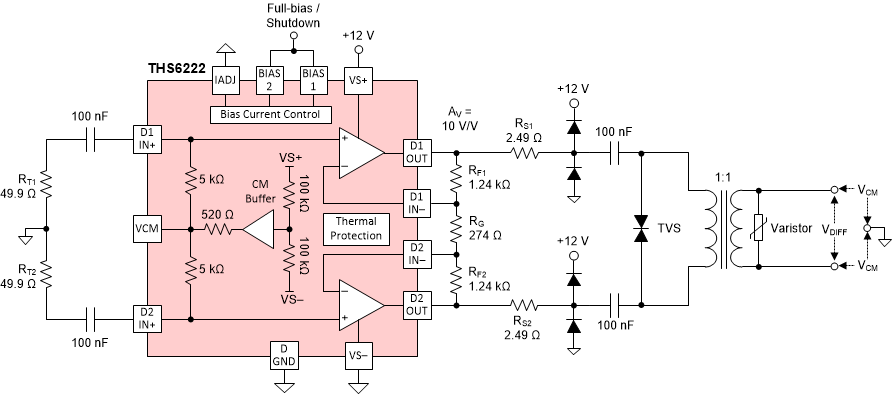 Figure 7-7 Surge Test
Configuration
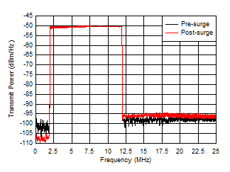 Figure 7-8 China SGCC HPLC Band0 Pre-Surge and Post-Surge
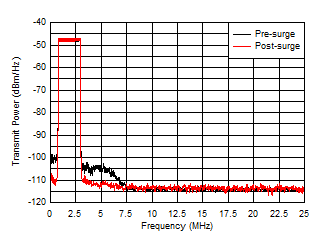 Figure 7-10 China SGCC HPLC Band2 Pre-Surge and Post-Surge
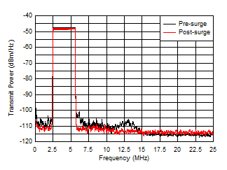 Figure 7-9 China SGCC HPLC Band1 Pre-Surge and Post-Surge
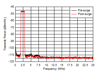 Figure 7-11 China SGCC HPLC Band3 Pre-Surge and Post-Surge