SBOS643A April 2014 – May 2014 THS6226A
PRODUCTION DATA.
- 1 Features
- 2 Applications
- 3 Description
- 4 Revision History
- 5 Pin Configuration and Functions
- 6 Specifications
- 7 Detailed Description
- 8 Applications and Implementation
- 9 Power Supply Recommendations
- 10Layout
- 11Device and Documentation Support
- 12Mechanical, Packaging, and Orderable Information
Package Options
Mechanical Data (Package|Pins)
- RHB|32
Thermal pad, mechanical data (Package|Pins)
- RHB|32
Orderable Information
7 Detailed Description
7.1 Overview
The THS6226A class H line driver provides exceptional ac performance in conjunction with wide output voltage swing. The class H operation allows voltage swings to exceed the power supply for short intervals limited only by the charge in the capacitor. In class AB mode, the device is capable of driving a 100-Ω load from +1.8 V to
+10.2 V. In class H mode, under the same conditions, the output voltage range becomes an impressive –5.5 V to +17.5 V, or 46 VPP differentially with the capacitor fully charged.
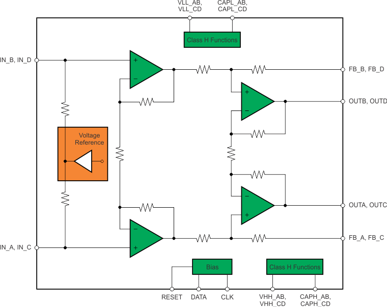
The Functional Block Diagram section shows a fully-differential, noninverting amplifier configuration with active impedance. In this configuration, the 10.2-Ω matching resistor appears through the transformer as 100 Ω, minimizing reflection on the line. This active impedance scheme also minimizes transmission losses, as compared to passive termination. Device gain is fixed and is equal to 19 V/V from the input to the output of the amplifier (INAB/CD to OUTAB/CD), not including the transformer-turn ratio or the termination loss.
To simplify the implementation as well as to provide design flexibility, the device contains an integrated mid-supply buffer that provides the correct biasing to the amplifier core without requiring any external components. Also present is a two-pin serial interface that provides exceptional design flexibility and allows minimal power consumption for each xDSL profile.
7.2 Functional Block Diagram
7.3 Feature Description
The device incorporates several hardware and functionality features: a high output current line driver, a charge pump, a voltage reference, a logic circuit, an active impedance, and a RESET pin. The device has two ports. Each port consists of a high output current line driver, a charge pump, and a reference voltage. Common circuits are the RESET feature and the logic circuit.
7.3.1 High Output Current Line Driver
The main purpose for the device is to provide a high output current into a heavy load. For the THS6226A, with its xDSL application targeted, the load is typically 100 Ω and currents as high as 400 mA are supported with excellent linearity. The core of the line driver is a class AB amplifier providing both good efficiency and high current drive capability. The high output line driver is the core of the device and any external circuit interface is located on both the device inputs and output.
7.3.2 Charge Pump
The class H functionality of the device is brought on by the integration of a charge pump. The charge pump is a power-supply function to the line driver. The role of the charge pump is to vary the power supply from (12 V / GND) to (20 V / –8 V) and allow the line driver to support high peak to average ratio (PAR) signals while minimizing power consumption and maintaining excellent linearity. The charge pump is controlled externally by the VH_EN pin. A logic high on the VH_EN pin results in the power supply of the class AB line driver going to (20 V / –8 V), while a logic low on the VH_EN pin results in normal operation under the (12 V / GND) supplies.
7.3.3 Voltage Reference
An internal voltage reference provides the device common-mode input and output voltage.
7.3.4 Logic
The DATA and CLK pins allow access to the internal logic circuit implemented in the device. This logic circuit allows each channel to either be programmed individually for quiescent current, turn the charge pump on or off, disable the main amplifier, or select the line termination mode. For more information on programming, refer to the Programming section.
7.3.5 Active Impedance
The line driver incorporates the positive feedback path to provide the termination to the load. For the device, the synthesis factor implemented is 5.
7.3.6 RESET Pin
The RESET pin provides a quick and easy way to disable the two ports immediately if a fault condition on the line occurs.
7.4 Device Functional Modes
There are several functional modes for the device. These functional modes can be accessed with the CLK and DATA pins. Each main line driver quiescent current can be set to 16 different bias modes: bias 0 through bias 15. Additionally, the line driver and class H feature can be controlled to have the following configuration:
- Class AB mode is the main line driver by itself. The output voltage is limited by the (12 V / GND) power-supply rails. The quiescent current is then set by four bits.
- Class H mode is the main line driver used in conjunction with the class H feature. The output voltage is limited by the (20 V / –8 V) internally-generated power-supply rails. The quiescent current of the main line driver is set by four bits, as in class AB mode.
- Line termination mode is the powered-down mode for the line driver. This mode maintains line termination but has reduced linearity performance.
- Disabled mode.
For more information on these mode, refer to the Programming section.
7.5 Programming
7.5.1 Programming the Device
Programming the device is accomplished through a serial interface (pins 4 and 5) and proceeds in the following sequence:
- Two start bits are required (B0 = 0 followed by B1 = 1).
- B2 through B9 are used to program the device. (Table 1 lists the bit descriptions.)
- B10 (described in Table 2) is the parity bit that controls whether the word is loaded or not.
- B11 is the stop bit and must be set to B11 = 1.
Figure 32 shows the required sequence.
Table 1. DATA Sequence
| PARAMETER | DESCRIPTION |
|---|---|
| B0, B1 | Start bits |
| B2, B3 | Channel select |
| B4, B5 | Power-down features |
| B6-B9 | Quiescent current setting |
| B10 | Parity bit |
| B11 | Stop bit |
Table 2. Parity Bit
| B10 | ODD PARITY BIT |
|---|---|
| 0 | For an odd number of high bits in B2 to B9, set B10 to 0 |
| 1 | For an even number of high bits in B2 to B9, set B10 to 1 |
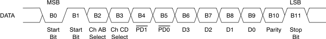 Figure 32. DATA Description
7.5.2 Quiescent Current
The device quiescent current is dissipated in two main device modules: the class AB and the charge pump. Bits B4 (PD1) and B5 (PD0) select one of the possible four modes of operation:
- Class AB mode (charge pump disabled),
- Class H mode (charge pump enabled),
- Disable mode, or
- Line termination mode (maintains line matching, core amplifier at very low bias mode and charge pump disabled for lowest power consumption possible).
Table 3 lists the details on each bit functionality and the approximate quiescent current. The various power modes are shown in Table 3. For all modes, when B6 through B9 are not defined, set B9 = B8 = B7 = B6 = 0 to achieve the lowest power dissipation possible.
Table 3. Power Modes
| B4 (PD1) | B5 (PD0) | POWER-DOWN MODE | APPROXIMATE IQ (mA per Port) |
|---|---|---|---|
| 0 | 0 | Power-down (B9 = B8 = B7 = B6 = 0) | 0.85 |
| 0 | 1 | Line termination mode (B9 = B8 = B7 = B6 = 0) | 4.4 |
| 1 | 0 | Class AB driver IQ set by B6 to B9, class H disabled | — |
| 1 | 1 | Class AB driver IQ set by B6 to B9, class H enabled | — |
The class AB quiescent current is set by bits B6 to B9, using B4 and B5 for the power-down function and B2 and B3 for channel selection. The approximate quiescent current for the amplifier core is shown in Table 4.
Table 4. Class AB Quiescent Current
| BIAS | B6 (D3) | B7 (D2) | B8 (D1) | B9 (D0) | QUIESCENT CURRENT SETTING | APPROXIMATE IQ (mA per Port) |
|---|---|---|---|---|---|---|
| 0 | 0 | 0 | 0 | 0 | 9.4 | |
| 1 | 0 | 0 | 0 | 1 | 10.4 | |
| 2 | 0 | 0 | 1 | 0 | ADSL2+ mode | 11.5 |
| 3 | 0 | 0 | 1 | 1 | 12.5 | |
| 4 | 0 | 1 | 0 | 0 | 13.6 | |
| 5 | 0 | 1 | 0 | 1 | 14.6 | |
| 6 | 0 | 1 | 1 | 0 | 15.7 | |
| 7 | 0 | 1 | 1 | 1 | Profile 8b mode | 16.7 |
| 8 | 1 | 0 | 0 | 0 | 17.8 | |
| 9 | 1 | 0 | 0 | 1 | 18.8 | |
| 10 | 1 | 0 | 1 | 0 | 19.8 | |
| 11 | 1 | 0 | 1 | 1 | Profile 17a mode | 20.8 |
| 12 | 1 | 1 | 0 | 0 | 21.8 | |
| 13 | 1 | 1 | 0 | 1 | 22.8 | |
| 14 | 1 | 1 | 1 | 0 | 23.8 | |
| 15 | 1 | 1 | 1 | 1 | 24.8 |
Channel selection is shown in Table 5. Each channel can be programmed independently, or together if both B2 and B3 are set to 1.
Table 5. Channel Selection
| B2 (Channel AB) | B3 (Channel CD) | CHANNEL SELECT |
|---|---|---|
| 0 | 0 | Bits B4 to B9 are ignored |
| 0 | 1 | Channel B programmed with B4 to B9 |
| 1 | 0 | Channel A programmed with B4 to B9 |
| 1 | 1 | Channels A and B programmed with B4 to B9 |
At startup, the internal register is set as shown in Figure 33.
| 7 | 6 | 5 | 4 | 3 | 2 | 1 | 0 |
| Ch. AB Select (B2) | Ch. CD Select (B3) | PD1(B4) | PD0(B5) | D3 (B6) | D2 (B7) | D1 (B8) | D0 (B9) |
| W | W | W | W | W | W | W | W |
| LEGEND: W = Write |
In this condition, the total quiescent power dissipation is 10.2 mW per port on a +12-V supply.