SBOS643A April 2014 – May 2014 THS6226A
PRODUCTION DATA.
- 1 Features
- 2 Applications
- 3 Description
- 4 Revision History
- 5 Pin Configuration and Functions
- 6 Specifications
- 7 Detailed Description
- 8 Applications and Implementation
- 9 Power Supply Recommendations
- 10Layout
- 11Device and Documentation Support
- 12Mechanical, Packaging, and Orderable Information
Package Options
Mechanical Data (Package|Pins)
- RHB|32
Thermal pad, mechanical data (Package|Pins)
- RHB|32
Orderable Information
6 Specifications
6.1 Absolute Maximum Ratings(1)
over operating free-air temperature range (unless otherwise noted)| MIN | MAX | UNIT | ||
|---|---|---|---|---|
| Supply voltage, GND to VS+ | Class AB only | 16.5 | V | |
| Class H only | 12.8 | V | ||
| Input voltage, VI | 15 | V | ||
| Output current, IO | Static dc(2) | ±100 | mA | |
| Continuous power dissipation | See Thermal Information table | |||
| Temperature | Maximum junction, any condition, TJ(3) | 150 | °C | |
| Maximum junction, continuous operation, long-term reliability, TJ(4) | 130 | °C | ||
(1) Stresses above those listed under absolute maximum ratings may cause permanent damage to the device. These are stress ratings only, and functional operation of the device at these or any other conditions beyond those indicated under recommended operating conditions is not implied. Exposure to absolute maximum rated conditions for extended periods may degrade device reliability.
(2) The device incorporates a PowerPAD on the underside of the chip, which functions as a heatsink and must be connected to a thermally dissipating plane for proper power dissipation. Failure to do so may result in exceeding the maximum junction temperature, which could permanently damage the device. See the technical brief PowerPAD™ Thermally Enhanced Package (SLMA002) for more information about using the PowerPAD thermally-enhanced package. Under high-frequency ac operation (> 10 kHz), the short-term output current capability is much greater than the continuous dc output current rating. This short-term output current rating is roughly 8.5 times the dc capability, or approximately ±850 mA.
(3) The absolute maximum junction temperature under any condition is limited by the constraints of the silicon process.
(4) The absolute maximum junction temperature for continuous operation is limited by the package constraints. Operation above this temperature may result in reduced reliability or lifetime of the device.
6.2 Handling Ratings
6.3 Recommended Operating Conditions
over operating free-air temperature range (unless otherwise noted)| MIN | NOM | MAX | UNIT | ||
|---|---|---|---|---|---|
| Power-supply voltage range | Class H | 10 | 12.6 | V | |
| Class AB | 10 | 15 | V | ||
| Operating junction temperature | –40 | 130 | °C | ||
6.4 Thermal Information
| THERMAL METRIC(1) | THS6226A | UNIT | |
|---|---|---|---|
| RHB (VQFN) | |||
| 32 PINS | |||
| RθJA | Junction-to-ambient thermal resistance | 35.1 | °C/W |
| RθJC(top) | Junction-to-case (top) thermal resistance | 22.1 | |
| RθJB | Junction-to-board thermal resistance | 7.0 | |
| ψJT | Junction-to-top characterization parameter | 0.3 | |
| ψJB | Junction-to-board characterization parameter | 6.9 | |
| RθJC(bot) | Junction-to-case (bottom) thermal resistance | 1.3 | |
(1) For more information about traditional and new thermal metrics, see the IC Package Thermal Metrics application report, SPRA953.
6.5 Electrical Characteristics: VS = +12 V
At TA = 25°C, RMATCH = 10.2 Ω, transformer turn ratio 1:1.4, RL = 100-Ω differential at transformer output, full bias mode, and active impedance circuit configuration, unless otherwise noted. Each port is tested independently.| PARAMETER | CONDITIONS | MIN | TYP | MAX | UNIT | TEST LEVEL(1) | ||
|---|---|---|---|---|---|---|---|---|
| AC PERFORMANCE | ||||||||
| Small-signal bandwidth, –3 dB | VO = 2 VPP, differential at OUTCD and OUTAB, gain = 19 V/V |
97 | MHz | C | ||||
| 0.1-dB bandwidth flatness | VO = 2 VPP | 30 | MHz | C | ||||
| Large-signal bandwidth | VO = 7.5 VPP | 80 | MHz | C | ||||
| SR | Slew rate (10% to 90% level) | VO = 15-V step, differential | 1750 | V/μs | C | |||
| Rise-and-fall time | VO = 2 VPP | 3.6 | ns | C | ||||
| HD2 | Second-harmonic distortion | Full bias, f = 1 MHz, VO = 2 VPP, RL = 60-Ω differential |
–87 | dBc | C | |||
| Full bias, f = 5 MHz, VO = 2 VPP, RL = 60-Ω differential |
–73 | dBc | C | |||||
| HD3 | Third-harmonic distortion | Full bias, f = 1 MHz, VO = 2 VPP, RL = 60-Ω differential |
–83 | dBc | C | |||
| Full bias, f = 5 MHz, VO = 2 VPP, RL = 60-Ω differential |
–71 | dBc | C | |||||
| Differential input voltage noise | f = 1 MHz, input-referred | 6.5 | nV/√Hz | C | ||||
| DC PERFORMANCE | ||||||||
| Differential gain | Closed-loop configuration | 19 | V/V | C | ||||
| Differential gain error(4) | TA = 25°C | ±8% | A | |||||
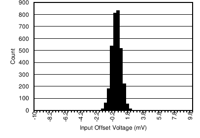
| VIO | Input offset voltage | TA = 25°C | ±1 | ±10 | mV | A | ||
| TA = –40°C to 85°C | ±11 | mV | B | |||||
| Input offset voltage drift | 15 | μV/°C | B | |||||
| Input offset voltage matching | Channels 1 to 2 and 3 to 4 only, TA = 25°C |
±1 | ±10 | mV | A | |||
| INPUT CHARACTERISTICS | ||||||||
| Noninverting input resistance | 2 || 2 | kΩ || pF | C | |||||
| Input bias voltage | TA = 25°C | 5.8 | 6 | 6.2 | V | A | ||
| OUTPUT CHARACTERISTICS | ||||||||
| Class H output | Voltage swing | RL = 60-Ω differential, class H operation(3)(5), each output, TA = 25°C | 16 | 17.5 | V | A | ||
| –4 | –5.5 | V | A | |||||
| TA = –40°C to 85°C(3)(5) | 15.7 | V | B | |||||
| –3.7 | V | B | ||||||
| Current (sourcing, sinking) |
RL = 60-Ω differential, class H operation, TA = 25°C | ±333 | ±383 | mA | A | |||
| TA = –40°C to 85°C | ±323 | mA | B | |||||
| Class AB output | Voltage swing | RL = 60-Ω differential, normal operation(3), each output, TA = 25°C | 9.9 | 10.1 | V | A | ||
| 2.1 | 1.9 | V | A | |||||
| TA = –40°C to 85°C(3) | 9.8 | V | B | |||||
| 2.2 | V | B | ||||||
| Current (sourcing, sinking) |
RL = 60-Ω differential, normal operation, TA = 25°C |
±130 | ±137 | mA | A | |||
| TA = –40°C to 85°C | ±126 | mA | B | |||||
| Short-circuit output current | 1 | A | C | |||||
| zo | Output impedance | f = 1 MHz, differential | 25 | Ω | C | |||
| Crosstalk | f = 1 MHz, VOUT = 2 VPP, port 1 to port 2 | –90 | dB | C | ||||
| POWER SUPPLY | ||||||||
| Maximum operating voltage | Class AB, TA = 25°C | 10 | 12 | 15 | V | A | ||
| TA = –40°C to 85°C | 10 | 15 | V | B | ||||
| Class H | 10 | 12 | 12.6 | V | B | |||
| TA = –40°C to 85°C | 10 | 12.6 | V | B | ||||
| IQ | Quiescent current (IS+) | Per port, bias 15, class H enable (power supplies connected together), TA = 25°C |
23.4 | 24.6 | 25.8 | mA | A | |
| TA = –40°C to 85°C | 22.9 | 26.1 | mA | B | ||||
| Per port, bias 15, class H disable (power supplies connected together), TA = 25°C |
22.8 | 24.0 | 25.2 | mA | A | |||
| TA = –40°C to 85°C | 22.3 | 25.7 | mA | B | ||||
| Bias current step | 1 | mA | C | |||||
| Per port, bias 0, class H disable (power supplies connected together), TA = 25°C |
8.5 | 9.7 | 10.9 | mA | A | |||
| TA = –40°C to 85°C | 8.0 | 11.4 | mA | B | ||||
| Per port, line termination mode (B9 = B8 = B7 = B6 = 0) (power supplies connected together) |
7.0 | mA | C | |||||
| Both ports, main amplifiers and class H disable (B9 = B8 = B7 = B6 = 0) |
1.9 | 2.4 | mA | A | ||||
| TA = –40°C to 85°C | 2.5 | mA | B | |||||
| PSRR | Power-supply rejection ratio | Differential, from 12 V, GND, TA = 25°C | 60 | 70 | dB | A | ||
| TA = –40°C to 85°C | 58 | dB | B | |||||
| LOGIC | ||||||||
| Logic pin | Logic threshold | Logic 1, with respect to GND(2) | 1.9 | V | C | |||
| Logic 0, with respect to GND(2) | 0.8 | V | C | |||||
| Input Bias current | Logic X = 0.5 V (logic 0), TA = 25°C | 10 | 25 | μA | A | |||
| TA = –40°C to 85°C | 30 | μA | B | |||||
| Logic X = 3.3 V (logic 1), TA = 25°C | 66 | 125 | μA | A | ||||
| TA = –40°C to 85°C | 130 | μA | B | |||||
| Input impedance | 50 || 1 | kΩ || pF | C | |||||
| td(on) | Turn-on time delay | Time for IS to reach 50% of final value | 1 | μs | C | |||
| td(off) | Turn-off time delay | Time for IS to reach 50% of final value | 1 | μs | C | |||
(1) Test levels: (A) 100% tested at 25°C. Overtemperature limits set by characterization and simulation. (B) Limits set by characterization and simulation. (C) Typical value only for information.
(2) The GND pin usable range is from VS– to (VS+ – 5 V).
(3) Measured at the amplifier outputs (pins 17, 20, 21, and 24).
(4) Negative feedback loop only.
(5) Capacitor fully charged, no droop.
6.6 Timing Characteristics
| PARAMETER | MIN | MAX | UNITS | |
|---|---|---|---|---|
| tCL | Clock period | 200 | ns | |
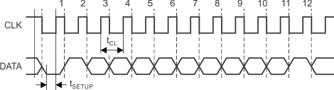 Figure 1. Serial Interface Timing
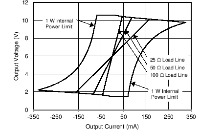
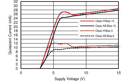
6.7 Typical Characteristics
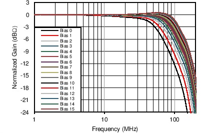
At TA = 25°C, 1:1.4 transformer, and 10.2-Ω matching resistance, unless otherwise noted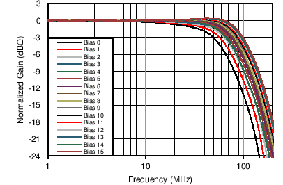
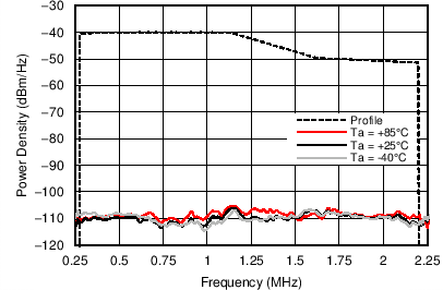
| VO = 2 VPP | ||
| 1:1.4 Transformer into 100 Ω | Bias 2 | |
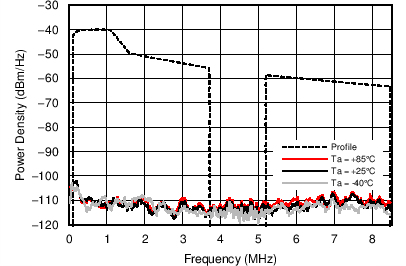
| ADSL | ||
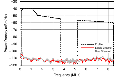
| 1:1.4 Transformer into 100 Ω | VDSL Profile 8 | |
| Bias 7 | ||
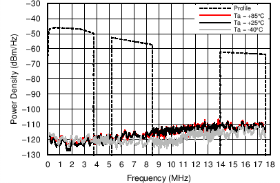
| 1:1.4 Transformer into 100 Ω | VDSL Profile 17 | |
| Bias 11 | ||
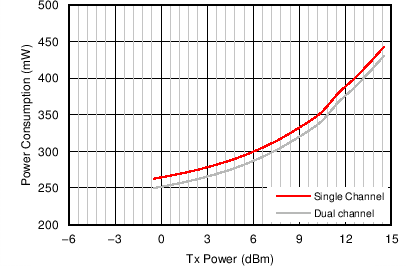
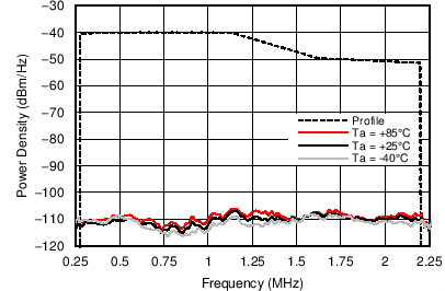
| 1:1.4 Transformer into 100 Ω | Bias 2 | |
| ADSL | ||
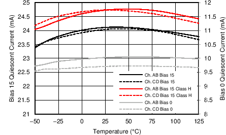
vs Temperature
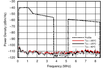
| 1:1.4 Transformer into 100 Ω | VDSL Profile 8 | |
| Bias 7 | ||
vs Temperature
| 1:1.4 Transformer into 100 Ω | VDSL Profile 17 | |
| Bias 11 | ||
vs Temperature
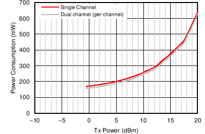
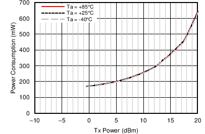
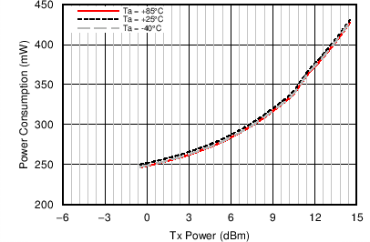
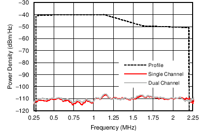
| 1:1.4 Transformer into 100 Ω | Bias 2 | |
| ADSL | Per Channel | |
vs Tx Power
| 1:1.4 Transformer into 100 Ω | Bias 7 | |
| VDSL Profile 8 | Per Channel | |
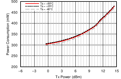
vs Temperature
| 1:1.4 Transformer into 100 Ω | Bias 11 | |
| VDSL Profile 17 | Per Channel | |
vs Temperature
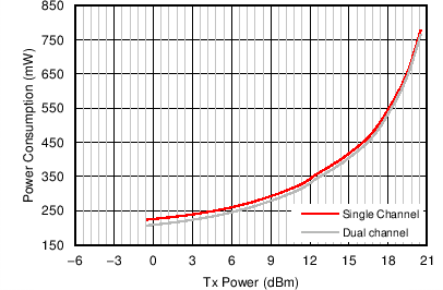
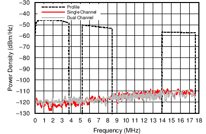
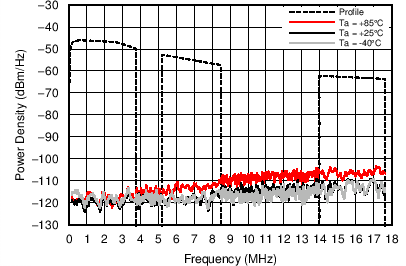
| 1:1.4 Transformer into 100 Ω | Bias 15 | |
| VDSL Profile 30 | ||
vs Temperature
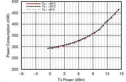
| Per Channel | ||
vs Temperature
| VO = 7.5 VPP | ||
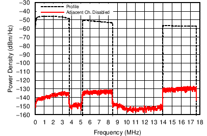
| 14.5-dBm Tx Power in One Channel | Bias 11 | |
| MTPR Measured on Adjacent channel | ||
| 19.8-dBm Tx Power | 1:1.4 Transformer into 100 Ω | |
| Bias 2 | ||
| 20.5-dBm Tx Power | 1:1.4 Transformer into 100 Ω | |
| Bias 7 | ||
| 14.5-dBm Tx Power | 1:1.4 Transformer into 100 Ω | |
| Bias 11 | ||
| 19.8-dBm Tx Power | 1:1.4 Transformer into 100 Ω | |
| Bias 2 | ||
| 20.5-dBm Tx Power | 1:1.4 Transformer into 100 Ω | |
| Bias 7 | ||
| 14.5-dBm Tx Power | 1:1.4 Transformer into 100 Ω | |
| Bias 11 | ||
| 19.8-dBm Tx Power | 1:1.4 Transformer into 100 Ω | |
| Bias 2 | ||
| 20.5-dBm Tx Power | 1:1.4 Transformer into 100 Ω | |
| Bias 7 | ||
| 14.5-dBm Tx Power | 1:1.4 Transformer into 100 Ω | |
| Bias 11 | ||
| 14.5-dBm Tx Power | 1:1.4 Transformer into 100 Ω | |
| Bias 15 | ||
| 14.5-dBm Tx Power | 1:1.4 Transformer into 100 Ω | |||
| Bias 15 | ||||