SLLSFD6A May 2020 – March 2021 THVD8000
PRODUCTION DATA
- 1 Features
- 2 Applications
- 3 Description
- 4 Revision History
- 5 Pin Configuration and Functions
- 6 Specifications
- 7 Parameter Measurement Information
- 8 Detailed Description
- 9 Application Information Disclaimer
- 10Power supply recommendations
- 11Layout
- 12Device and Documentation Support
Package Options
Mechanical Data (Package|Pins)
- DDF|8
Thermal pad, mechanical data (Package|Pins)
Orderable Information
9.2 Typical application (OOK mode)
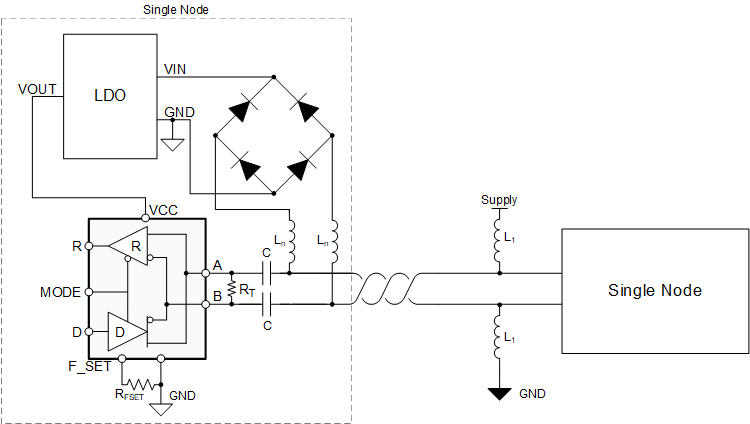
In order to combine data and power over a single pair of wires, capacitors and inductors are used in a bias-tee configuration. High-frequency differential data is AC-coupled onto the bus lines via series capacitances while power is DC-coupled via series inductances. The values of these components will depend on the carrier frequency, number of nodes on the bus, and the power delivery requirements (i.e., voltage and total current sourced or consumed by a given node).
The transmitted differential communication signal is AC-coupled onto the power bus as shown below. This configuration provides the advantage that the power transmitted on the bus has little impact on the differential data, allowing for a wide range of voltage and current scenarios. Typical applications are realized with the THVD8000 transmitting over a power bus of 24VDC or 24VAC with currents from 100mA to 1A, but due to the AC-coupling the THVD8000 does not directly see these voltages. For more information, please refer for the THVD8000 design guide.
In Figure 9-1, there is an optional rectifier network pictured on the bus lines. This network of diodes can ensure that the node is receives power correctly from the bus wires, even if the lines get swapped.
A termination resistance, RT, is not required for device functionality but can be useful in improving signal integrity in some applications by reducing reflections that can occur at cable ends.
 Figure 9-1 Typical power line network with 2 nodes