SLVS641B April 2008 – March 2015 TL4242
PRODUCTION DATA.
- 1 Features
- 2 Applications
- 3 Description
- 4 Revision History
- 5 Pin Configuration and Functions
- 6 Specifications
- 7 Detailed Description
- 8 Application and Implementation
- 9 Power Supply Recommendations
- 10Layout
- 11Device and Documentation Support
- 12Mechanical, Packaging, and Orderable Information
Package Options
Mechanical Data (Package|Pins)
- DRJ|8
Thermal pad, mechanical data (Package|Pins)
- DRJ|8
Orderable Information
7 Detailed Description
7.1 Overview
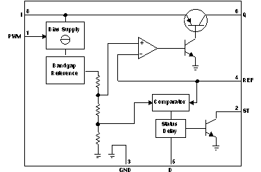
The TL4242 device is an integrated, adjustable, constant-current source that can drive loads up to 500 mA. The output current level can be adjusted through an external resistor. The device is designed to supply high-power LEDs. Protection circuits prevent damage to the device in case of overload, short circuit, reverse polarity, and overtemperature. The connected LEDs are protected against reverse polarity as well as excess voltages up to 45 V. The integrated PWM input of the TL4242 permits LED brightness regulation by pulse-width modulation (PWM). Due to the high input impedance of the PWM input, the LED driver can be operated as a protected high-side switch.
7.2 Functional Block Diagram

7.3 Feature Description
7.3.1 PWM Input
The integrated PWM input of the TL4242 permits LED brightness regulation by pulse-width modulation (PWM). The overall LED brightness is a function of the shunt resistor, RREF, and the PWM duty cycle. The PWM input can also function as a simple enable control. When the PWM input is below VPWM,L, the device will go to a low-power consumption sleep mode. Due to the high input impedance of the PWM input, the LED driver can be operated as a protected high-side switch.
The LEDs are driven by a supply current that is adjusted by the resistor, RREF, preventing brightness variations due to forward voltage spread of the LEDs. The luminosity spread arising from the LED production process can be compensated through software by an appropriate duty cycle applied to the PWM pin. Therefore, it is not necessary to select LEDs for forward voltage or luminosity classes.
7.3.2 ST Output
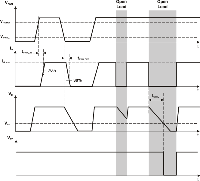
The status output of the LED driver (ST) detects an open-load condition, enabling supervision of correct LED operation. An LED failure is detected as a voltage drop at the shunt resistor (RREF) below 25 mV (typical). In this case, the status output pin (ST) is set low after a delay time adjustable by an optional capacitor connected to pin D.
7.3.2.1 Function and Timing Diagram
The functionality and timing of ST and PWM are shown in Figure 5. The status delay can be adjusted through the capacitor connected to pin D. Delay time scales linearly with capacitance, CD:


 Figure 5. Function and Timing Diagram
7.4 Device Functional Modes
Table 1. Functional Modes
| VPWM | DEVICE MODE | |||
|---|---|---|---|---|
| High | Active | |||
| Low | Sleep | |||