SLVS641B April 2008 – March 2015 TL4242
PRODUCTION DATA.
- 1 Features
- 2 Applications
- 3 Description
- 4 Revision History
- 5 Pin Configuration and Functions
- 6 Specifications
- 7 Detailed Description
- 8 Application and Implementation
- 9 Power Supply Recommendations
- 10Layout
- 11Device and Documentation Support
- 12Mechanical, Packaging, and Orderable Information
Package Options
Mechanical Data (Package|Pins)
- DRJ|8
Thermal pad, mechanical data (Package|Pins)
- DRJ|8
Orderable Information
5 Pin Configuration and Functions
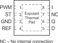
DRJ Package
8-Pin WSON
(Top View)

Pin Functions
| PIN | I/O | DESCRIPTION | |
|---|---|---|---|
| NO. | NAME | ||
| 1 | PWM | I | Pulse-width modulation input. If not used, connect to I. |
| 2 | ST | O | Status output. Open-collector output. Connect to an external pullup resistor (RPULLUP ≥ 4.7 kΩ). |
| 3 | GND | — | Ground |
| 4 | REF | I | Reference input. Connect to a shunt resistor. |
| 5 | D | I | Status delay. To set status reaction delay, connect to GND with a capacitor. If no delay is needed, leave open. |
| 6 | Q | O | Output |
| 7 | NC | — | No internal connection |
| 8 | I | I | Input. Connect directly to GND as close as possible to the device with a 100-nF ceramic capacitor. |
| — | Thermal Pad | — | The thermal pad must be soldered directly to the PCB. It may be connected to ground or left floating. |