SGLS156F March 2003 – December 2016 TLC3702-Q1
PRODUCTION DATA.
- 1 Features
- 2 Applications
- 3 Description
- 4 Revision History
- 5 Pin Configuration and Functions
- 6 Specifications
- 7 Parameter Measurement Information
- 8 Detailed Description
- 9 Application and Implementation
- 10Power Supply Recommendations
- 11Layout
- 12Device and Documentation Support
- 13Mechanical, Packaging, and Orderable Information
Package Options
Refer to the PDF data sheet for device specific package drawings
Mechanical Data (Package|Pins)
- D|8
- PW|8
Thermal pad, mechanical data (Package|Pins)
Orderable Information
8 Detailed Description
8.1 Overview
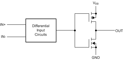
The TLC3702-Q1 push-pull output comparator features a low quiescent current 20 uA and operation from 4 V to 16 V. The push-pull CMOS output stage drives capacitive loads directly without a power consuming pull-up resistor to achieve the stated response time.
8.2 Functional Block Diagram
8.3 Feature Description
8.3.1 LinCMOS™ Process
The LinCMOS process is a linear polysilicon-gate CMOS process. Primarily designed for single-supply applications, LinCMOS products facilitate the design of a wide range of high-performance analog functions from operational amplifiers to complex mixed-mode converters.
While digital designers are experienced with CMOS, MOS technologies are relatively new for analog designers. This short guide is intended to answer the most frequently asked questions related to the quality and reliability of LinCMOS products. Further questions should be directed to the nearest TI field sales office.
8.3.2 Electrostatic Discharge
CMOS circuits are prone to gate oxide breakdown when exposed to high voltages even if the exposure is only for very short periods of time. Electrostatic discharge (ESD) is one of the most common causes of damage to CMOS devices. It can occur when a device is handled without proper consideration for environmental electrostatic charges, for example, during board assembly. If a circuit in which one amplifier from a dual op amp is being used and the unused pins are left open, high voltages tend to develop. If there is no provision for ESD protection, these voltages may eventually punch through the gate oxide and cause the device to fail. To prevent voltage buildup, each pin is protected by internal circuitry.
Standard ESD-protection circuits effectively shunt the ESD current by providing a mechanism whereby one or more transistors break down at voltages higher than the normal operating voltages but lower than the breakdown voltage of the input gate. This type of protection scheme is limited by leakage currents which flow through the shunting transistors during normal operation after an ESD voltage has occurred. Although these currents are small, on the order of tens of nanoamps, CMOS amplifiers are often specified to draw input currents as low as tens of picoamps.
To overcome this limitation, TI design engineers developed the patented ESD-protection circuit shown in Figure 21. This circuit can withstand several successive 2-kV ESD pulses, while reducing or eliminating leakage currents that may be drawn through the input pins. A more detailed discussion of the operation of the TI ESD-protection circuit is presented in the following sections.
All input and output pins on LinCMOS and Advanced LinCMOS products have associated ESD-protection circuitry that undergoes qualification testing to withstand 2000 V discharged from a 100-pF capacitor through a 1500-Ω resistor (human body model) and 200 V from a 100-pF capacitor with no current-limiting resistor (charged device model). These tests simulate both operator and machine handling of devices during normal test and assembly operations.
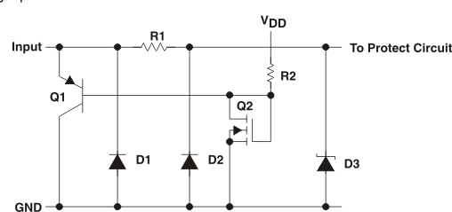 Figure 21. LinCMOS™ ESD-Protection Schematic
8.3.3 Input Protection Circuit Operation
TI's patented protection circuitry allows for both positive- and negative-going ESD transients. These transients are characterized by extremely fast rise times and usually low energies, and can occur both when the device has all pins open and when it is installed in a circuit.
8.3.4 Positive ESD Transients
Initial positive charged energy is shunted through Q1 to VSS. Q1 turns on when the voltage at the input rises above the voltage on the VDD pin by a value equal to the VBE of Q1. The base current increases through R2 with input current as Q1 saturates. The base current through R2 forces the voltage at the drain and gate of Q2 to exceed its threshold level (VT ∼ 22 to 26 V) and turn Q2 on. The shunted input current through Q1 to VSS is now shunted through the N-channel enhancement-type MOSFET Q2 to VSS. If the voltage on the input pin continues to rise, the breakdown voltage of the zener diode D3 is exceeded and all remaining energy is dissipated in R1 and D3. The breakdown voltage of D3 is designed to be 24 V to 27 V, which is well below the gate-oxide voltage of the circuit to be protected.
8.3.5 Negative ESD Transients
The negative charged ESD transients are shunted directly through D1. Additional energy is dissipated in R1 and D2 as D2 becomes forward biased. The voltage seen by the protected circuit is −0.3 V to −1 V (the forward voltage of D1 and D2).
8.3.6 Circuit-Design Considerations
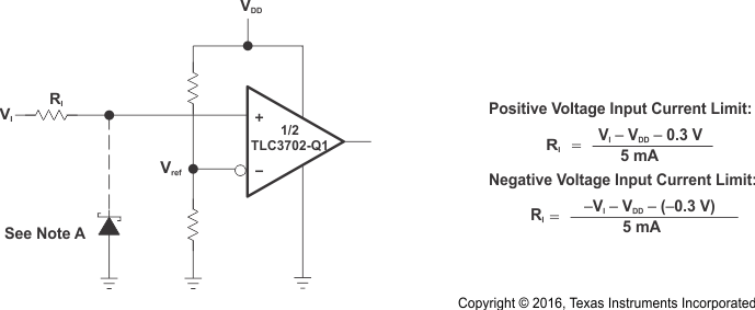
LinCMOS products are being used in actual circuit environments that have input voltages that exceed the recommended common-mode input voltage range and activate the input protection circuit. Even under normal operation, these conditions occur during circuit power up or power down, and in many cases, when the device is being used for a signal conditioning function. The input voltages can exceed VICR and not damage the device only if the inputs are current limited. The recommended current limit shown on most product data sheets is ±5 mA. Figure 22 and Figure 23 show typical characteristics for input voltage versus input current.
Normal operation and correct output state can be expected even when the input voltage exceeds the positive supply voltage. Again, the input current should be externally limited even though internal positive current limiting is achieved in the input protection circuit by the action of Q1. When Q1 is on, it saturates and limits the current to approximately 5-mA collector current by design. When saturated, Q1 base current increases with input current. This base current is forced into the VDD pin and into the device IDD or the VDD supply through R2 producing the current limiting effects shown in Figure 22. This internal limiting lasts only as long as the input voltage is below the VT of Q2.
When the input voltage exceeds the negative supply voltage, normal operation is affected and output voltage states may not be correct. Also, the isolation between channels of multiple devices (duals and quads) can be severely affected. External current limiting must be used since this current is directly shunted by D1 and D2 and no internal limiting is achieved. If normal output voltage states are required, an external input voltage clamp is required (see Figure 24).
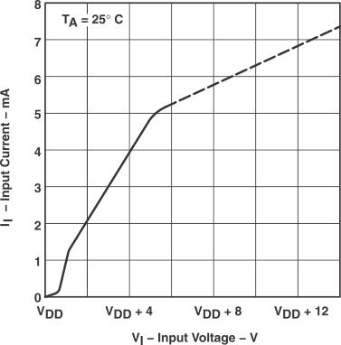 Figure 22. Input Current vs Input Voltage
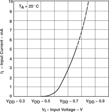 Figure 23. Input Current vs Input Voltage
8.4 Device Functional Modes
The TLC3702-Q1 is powered on when the supply is connected. The device can operate with single or dual supply, depending on the application. The device is in its full performance once the supply is above the recommended value.