SLDS162B March 2009 – December 2015 TLC59108F
PRODUCTION DATA.
- 1 Features
- 2 Applications
- 3 Description
- 4 Revision History
- 5 Pin Configuration and Functions
- 6 Specifications
- 7 Parameter Measurement Information
-
8 Detailed Description
- 8.1 Overview
- 8.2 Functional Block Diagram
- 8.3 Feature Description
- 8.4 Device Functional Modes
- 8.5 Programming
- 8.6
Register Maps
- 8.6.1 Control Register
- 8.6.2 Mode Register 1 (MODE1)
- 8.6.3 Mode Register 2 (MODE2)
- 8.6.4 Individual Brightness Control Registers (PWM0-PWM7)
- 8.6.5 Group Duty Cycle Control Register (GRPPWM)
- 8.6.6 Group Frequency Register (GRPFREQ)
- 8.6.7 LED Driver Output State Registers (LEDOUT0, LEDOUT1)
- 8.6.8 I2C Bus Sub-Address Registers 1 to 3 (SUBADR1-SUBADR3)
- 8.6.9 LED All Call I2C Bus Address Register (ALLCALLADR)
- 9 Application and Implementation
- 10Power Supply Recommendations
- 11Layout
- 12Device and Documentation Support
- 13Mechanical, Packaging, and Orderable Information
Package Options
Mechanical Data (Package|Pins)
- PW|20
Thermal pad, mechanical data (Package|Pins)
Orderable Information
11 Layout
11.1 Layout Guidelines
The I2C signals (SDA / SCL) should be kept away from potential noise sources.
The traces carrying power through the LEDS should be wide enough to handle the necessary current.
All LED current passes through the device and into the ground node. There must be a strong connection between the device ground and the circuit board ground. For the RGY package, the thermal pad should be connected to ground to help dissipate heat.
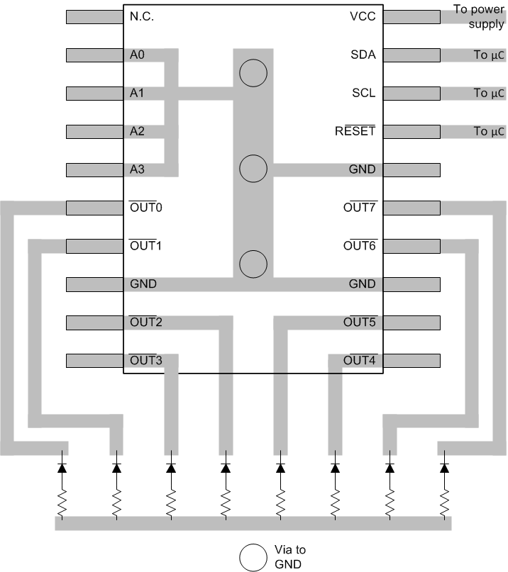
11.2 Layout Example
 Figure 25. RGY Layout Example
 Figure 26. PW Layout Example