SLDS162B March 2009 – December 2015 TLC59108F
PRODUCTION DATA.
- 1 Features
- 2 Applications
- 3 Description
- 4 Revision History
- 5 Pin Configuration and Functions
- 6 Specifications
- 7 Parameter Measurement Information
-
8 Detailed Description
- 8.1 Overview
- 8.2 Functional Block Diagram
- 8.3 Feature Description
- 8.4 Device Functional Modes
- 8.5 Programming
- 8.6
Register Maps
- 8.6.1 Control Register
- 8.6.2 Mode Register 1 (MODE1)
- 8.6.3 Mode Register 2 (MODE2)
- 8.6.4 Individual Brightness Control Registers (PWM0-PWM7)
- 8.6.5 Group Duty Cycle Control Register (GRPPWM)
- 8.6.6 Group Frequency Register (GRPFREQ)
- 8.6.7 LED Driver Output State Registers (LEDOUT0, LEDOUT1)
- 8.6.8 I2C Bus Sub-Address Registers 1 to 3 (SUBADR1-SUBADR3)
- 8.6.9 LED All Call I2C Bus Address Register (ALLCALLADR)
- 9 Application and Implementation
- 10Power Supply Recommendations
- 11Layout
- 12Device and Documentation Support
- 13Mechanical, Packaging, and Orderable Information
Package Options
Mechanical Data (Package|Pins)
- PW|20
Thermal pad, mechanical data (Package|Pins)
Orderable Information
7 Parameter Measurement Information
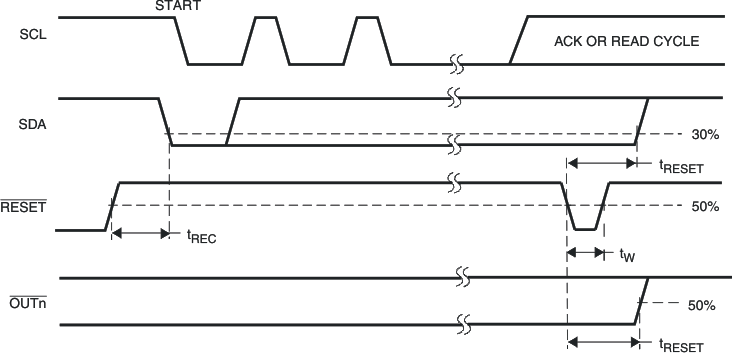
 Figure 3. Definition of Reset Timing
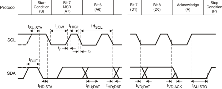
 Figure 4. Definition of Timing

Rise and fall times refer to VIL and VIH.
Figure 5. I2C Bus Timing

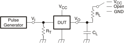
RL = Load resistance for SDA and SCL; should be >1 kΩ at 3-mA or lower current.
CL = Load capacitance; includes jig and probe capacitance.
RT = Termination resistance; should be equal to the output impedance (ZO) of the pulse generator.
Figure 6. Test Circuit for Switching Characteristics
CL = Load capacitance; includes jig and probe capacitance.
RT = Termination resistance; should be equal to the output impedance (ZO) of the pulse generator.