SLDS223A March 2016 – March 2016 TLC59116-Q1
PRODUCTION DATA.
- 1 Features
- 2 Applications
- 3 Description
- 4 Revision History
- 5 Description (continued)
- 6 Pin Configuration and Functions
- 7 Specifications
- 8 Parameter Measurement Information
-
9 Detailed Description
- 9.1 Overview
- 9.2 Functional Block Diagram
- 9.3 Feature Description
- 9.4 Device Functional Modes
- 9.5 Programming
- 9.6
Register Maps
- 9.6.1 Mode Register 1 (MODE1)
- 9.6.2 Mode Register 2 (MODE2)
- 9.6.3 Brightness Control Registers 0 to 15 (PWM0 to PWM15)
- 9.6.4 Group Duty Cycle Control Register (GRPPWM)
- 9.6.5 Group Frequency Register (GRPFREQ)
- 9.6.6 LED Driver Output State Registers 0 to 3 (LEDOUT0 to LEDOUT3)
- 9.6.7 I2C Bus Subaddress Registers 1 to 3 (SUBADR1 to SUBADR3)
- 9.6.8 LED All Call I2C Bus Address Register (ALLCALLADR)
- 9.6.9 Output Gain Control Register (IREF)
- 9.6.10 Error Flags Registers (EFLAG1, EFLAG2)
- 10Application and Implementation
- 11Power Supply Recommendations
- 12Layout
- 13Device and Documentation Support
- 14Mechanical, Packaging, and Orderable Information
Package Options
Mechanical Data (Package|Pins)
- PW|28
Thermal pad, mechanical data (Package|Pins)
- PW|28
Orderable Information
7 Specifications
7.1 Absolute Maximum Ratings
over operating free-air temperature (unless otherwise noted) (1)| MIN | MAX | UNIT | |||
|---|---|---|---|---|---|
| VCC | Supply voltage | 0 | 7 | V | |
| VI | Input voltage | –0.4 | VCC + 0.4 | V | |
| VO | Output voltage | –0.5 | 20 | V | |
| IO | Output current per channel | 120 | mA | ||
| TJ | Junction temperature | –40 | 150 | °C | |
| Tstg | Storage temperature | –55 | 150 | °C | |
(1) Stresses beyond those listed under Absolute Maximum Ratings may cause permanent damage to the device. These are stress ratings only, which do not imply functional operation of the device at these or any other conditions beyond those indicated under Recommended Operating Conditions. Exposure to absolute-maximum-rated conditions for extended periods may affect device reliability.
7.2 ESD Ratings
| VALUE | UNIT | |||
|---|---|---|---|---|
| V(ESD) | Electrostatic discharge | Human-body model (HBM), per AEC Q100-002(1) | ±2000 | V |
| Charged-device model (CDM), per AEC Q100-011 | ±1500 | |||
(1) AEC Q100-002 indicates that HBM stressing shall be in accordance with the ANSI/ESDA/JEDEC JS-001 specification.
7.3 Recommended Operating Conditions
All unused inputs of the device must be held at VCC or GND to ensure proper device operation| MIN | MAX | UNIT | ||||
|---|---|---|---|---|---|---|
| VCC | Supply voltage | 3 | 5.5 | V | ||
| VIH | High-level input voltage | SCL, SDA, RESET, A0, A1, A2, A3 | 0.7 × VCC | VCC | V | |
| VIL | Low-level input voltage | SCL, SDA, RESET, A0, A1, A2, A3 | 0 | 0.3 × VCC | V | |
| VO | Supply voltage to output pins | OUT0 to OUT15 | 17 | V | ||
| IOL | Low-level output current sink | SDA | VCC = 3 V | 20 | mA | |
| VCC = 5 V | 30 | |||||
| IO | Output current per channel | OUT0 to OUT15 | 5 | 120 | mA | |
| TA | Operating free-air temperature | –40 | 105 | °C | ||
7.4 Thermal Information
| THERMAL METRIC (1) | TLC59116-Q1 | UNIT | |
|---|---|---|---|
| PW (TSSOP) | |||
| 28 PINS | |||
| RθJA | Junction-to-ambient thermal resistance | 78 | °C/W |
| RθJC(top) | Junction-to-case (top) thermal resistance | 18.8 | °C/W |
| RθJB | Junction-to-board thermal resistance | 36 | °C/W |
| ψJT | Junction-to-top characterization parameter | 0.5 | °C/W |
| ψJB | Junction-to-board characterization parameter | 35.5 | °C/W |
| RθJC(bot) | Junction-to-case (bottom) thermal resistance | n/a | °C/W |
(1) For more information about traditional and new thermal metrics, see the Semiconductor and IC Package Thermal Metrics application report, SPRA953.
7.5 Electrical Characteristics
VCC = 3 V to 5.5 V, TA = –40°C to +105°C (unless otherwise noted)| PARAMETER | TEST CONDITIONS | MIN | TYP (1) | MAX | UNIT | |||
|---|---|---|---|---|---|---|---|---|
| II | Input / output leakage current | SCL, SDA, A0, A1, A2, A3, RESET | VI = VCC or GND | ±0.3 | μA | |||
| Output leakage current | OUT0 to OUT15 | VO = 17 V, TJ = 25°C | 0.5 | μA | ||||
| VPOR | Power-on reset voltage | 2.5 | V | |||||
| IOL | Low-level output current | SDA | VCC = 3 V, VOL = 0.4 V | 20 | mA | |||
| VCC = 5 V, VOL = 0.4 V | 30 | |||||||
| IO(1) | Output current 1 | OUT0 to OUT15 | VO = 0.6 V, Rext = 720 Ω, CG = 0.992 (3) | 26 | mA | |||
| Output current error | OUT0 to OUT15 | IO = 26 mA, VO = 0.6 V, Rext = 720 Ω, TJ = 25°C | ±10% | |||||
| Output channel to channel current error | OUT0 to OUT15 | IO = 26 mA, VO = 0.6 V, Rext = 720 Ω, TJ = 25°C | ±6% | |||||
| IO(2) | Output current 2 | OUT0 to OUT15 | VO = 0.8 V, Rext = 360 Ω, CG = 0.992 (3) | 52 | mA | |||
| Output current error | OUT0 to OUT15 | IO = 52 mA, VO = 0.8 V, Rext = 360 Ω, TJ = 25°C | ±8% | |||||
| Output channel to channel current error | OUT0 to OUT15 | IO = 52 mA, VO = 0.8 V, Rext = 360 Ω, TJ = 25°C | ±6% | |||||
| IOUT vs VOUT | Output current vs output voltage regulation | OUT0 to OUT15 | VO = 1 V to 3 V, IO = 26 mA | ±0.1 | %/V | |||
| VO = 3 V to 5.5 V, IO = 26 mA to 120 mA | ±1 | |||||||
| IOUT,Th1 | Threshold current 1 for error detection | OUT0 to OUT15 | IOUT,target = 26 mA | 0.5 × ITARGET% | ||||
| IOUT,Th2 | Threshold current 2 for error detection | OUT0 to OUT15 | IOUT,target = 52 mA | 0.5 × ITARGET% | ||||
| IOUT,Th3 | Threshold current 3 for error detection | OUT0 to OUT15 | IOUT,target = 104 mA | 0.5 × ITARGET% | ||||
| TSD | Overtemperature shutdown (2) | 150 | 175 | 200 | °C | |||
| THYS | Restart hysteresis | 15 | °C | |||||
| Ci | Input capacitance | SCL, A0, A1, A2, A3, RESET | VI = VCC or GND | 5 | pF | |||
| Cio | Input / output capacitance | SDA | VI = VCC or GND | 8 | pF | |||
| ICC | Supply current | VCC = 5.5 V | OUT0 to OUT15 = OFF, Rext = Open | 25 | mA | |||
| OUT0 to OUT15 = OFF, Rext = 720 Ω | 29 | |||||||
| OUT0 to OUT15 = OFF, Rext = 360 Ω | 32 | |||||||
| OUT0 to OUT15 = OFF, Rext = 180 Ω | 37 | |||||||
| OUT0 to OUT15 = ON, Rext = 720 Ω | 29 | |||||||
| OUT0 to OUT15 = ON, Rext = 360 Ω | 32 | |||||||
| OUT0 to OUT15 = ON, Rext = 180 Ω | 37 | |||||||
(1) All typical values are at TA = 25°C.
(2) Specified by design
(3) CG is the Current Gain and is defined in Table 13.
7.6 Timing Requirements
TA = –40°C to +105°C| I2C BUS | MIN | MAX | UNIT | ||
|---|---|---|---|---|---|
| I2C INTERFACE | |||||
| fSCL | SCL clock frequency (1) | STANDARD MODE | 0 | 100 | kHz |
| FAST MODE | 0 | 400 | |||
| FAST MODE PLUS | 0 | 1000 | |||
| tBUF | I2C Bus free time between Stop and Start conditions | STANDARD MODE | 4.7 | μs | |
| FAST MODE | 1.3 | ||||
| FAST MODE PLUS | 0.5 | ||||
| tHD;STA | Hold time (repeated) Start condition | STANDARD MODE | 4 | μs | |
| FAST MODE | 0.6 | ||||
| FAST MODE PLUS | 0.26 | ||||
| tSU;STA | Set-up time for a repeated Start condition | STANDARD MODE | 4.7 | μs | |
| FAST MODE | 0.6 | ||||
| FAST MODE PLUS | 0.26 | ||||
| tSU;STO | Set-up time for Stop condition | STANDARD MODE | 4 | μs | |
| FAST MODE | 0.6 | ||||
| FAST MODE PLUS | 0.26 | ||||
| tHD;DAT | Data hold time | STANDARD MODE | 0 | ns | |
| FAST MODE | 0 | ||||
| FAST MODE PLUS | 0 | ||||
| tVD;ACK | Data valid acknowledge time (2) | STANDARD MODE | 0.3 | 3.45 | μs |
| FAST MODE | 0.1 | 0.9 | |||
| FAST MODE PLUS | 0.05 | 0.45 | |||
| tVD;DAT | Data valid time (3) | STANDARD MODE | 0.3 | 3.45 | μs |
| FAST MODE | 0.1 | 0.9 | |||
| FAST MODE PLUS | 0.05 | 0.45 | |||
| tSU;DAT | Data set-up time | STANDARD MODE | 250 | ns | |
| FAST MODE | 100 | ||||
| FAST MODE PLUS | 50 | ||||
| tLOW | Low period of SCL clock | STANDARD MODE | 4.7 | μs | |
| FAST MODE | 1.3 | ||||
| FAST MODE PLUS | 0.5 | ||||
| tHIGH | High period of SCL clock | STANDARD MODE | 4 | μs | |
| FAST MODE | 0.6 | ||||
| FAST MODE PLUS | 0.26 | ||||
| tf | Fall time of both SDA and SCL signals (5) (6) | STANDARD MODE | 300 | ns | |
| FAST MODE | 20+0.1Cb (4) | 300 | |||
| FAST MODE PLUS | 120 | ||||
| tr | Rise time of both SDA and SCL signals | STANDARD MODE | 1000 | ns | |
| FAST MODE | 20+0.1Cb (4) | 300 | |||
| FAST MODE PLUS | 120 | ||||
| tSP | Pulse width of spikes that must be suppressed by the input filter (7) | STANDARD MODE | 50 | ns | |
| FAST MODE | 50 | ||||
| FAST MODE PLUS | 50 | ||||
| RESET | |||||
| tW | Reset pulse width | STANDARD MODE | 10 | ns | |
| FAST MODE | 10 | ||||
| FAST MODE PLUS | 10 | ||||
| tREC | Reset recovery time | STANDARD MODE | 0 | ns | |
| FAST MODE | 0 | ||||
| FAST MODE PLUS | 0 | ||||
| tRESET | Time to reset (8) (9) | STANDARD MODE | 400 | ns | |
| FAST MODE | 400 | ||||
| FAST MODE PLUS | 400 | ||||
(1) The TLC59116-Q1 does not have a self timeout on the I2C Bus. The Master can issue a reset if needed.
(2) tVD;ACK = time for ACK signal from SCL low to SDA (out) low.
(3) tVD;DAT = minimum time for SDA data out to be valid following SCL low.
(4) Cb = Total capacitance of one bus line in pF
(5) A master device must internally provide a hold time of at least 300 ns for the SDA signal (refer to the VIL of the SCL signal) in order to bridge the undefined region of the SCL falling edge.
(6) The maximum tf for the SDA and SCL bus lines is specified at 300 ns. The maximum fall time (tf) for the SDA output stage is specified at 250 ns. This allows series protection resistors to be connected between the SDA and the SCL pins and the SDA/SCL bus lines without exceeding the maximum specified tf.
(7) Input filters on the SDA and SCL inputs suppress noise spikes less than 50 ns.
(8) Resetting the device while actively communicating on the bus may cause glitches or errant Stop conditions.
(9) Upon reset, the full delay will be the sum of tRESET and the RC time constant of the SDA bus.
7.7 Typical Characteristics

A.
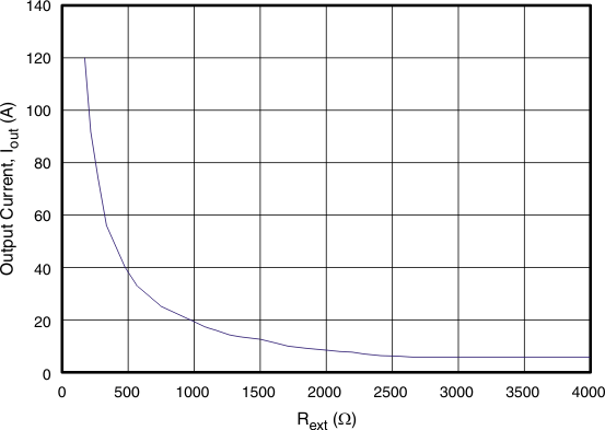
Figure 1. IOUT,target vs Rext

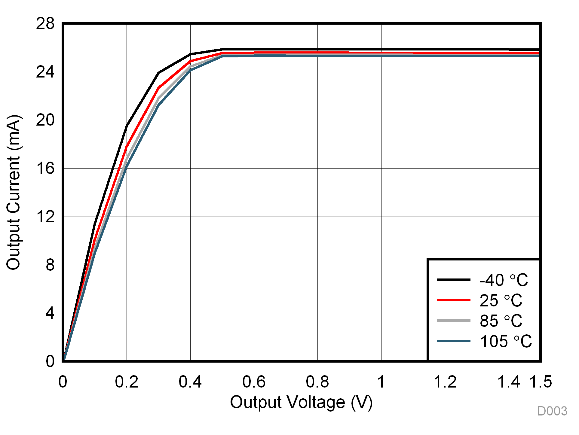
| VCC = 5 V | CG = 0.992 | REXT = 720 Ω |

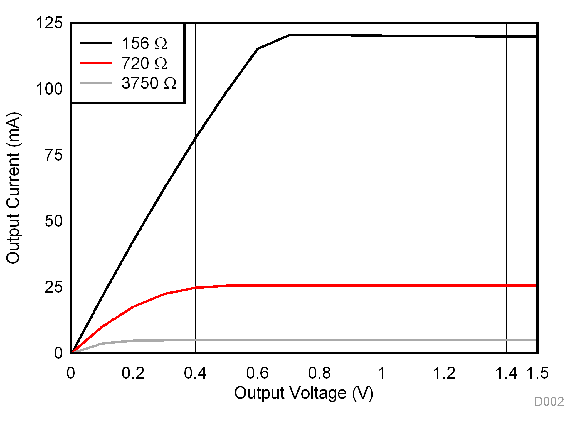
| VCC = 5 V | CG = 0.992 | |

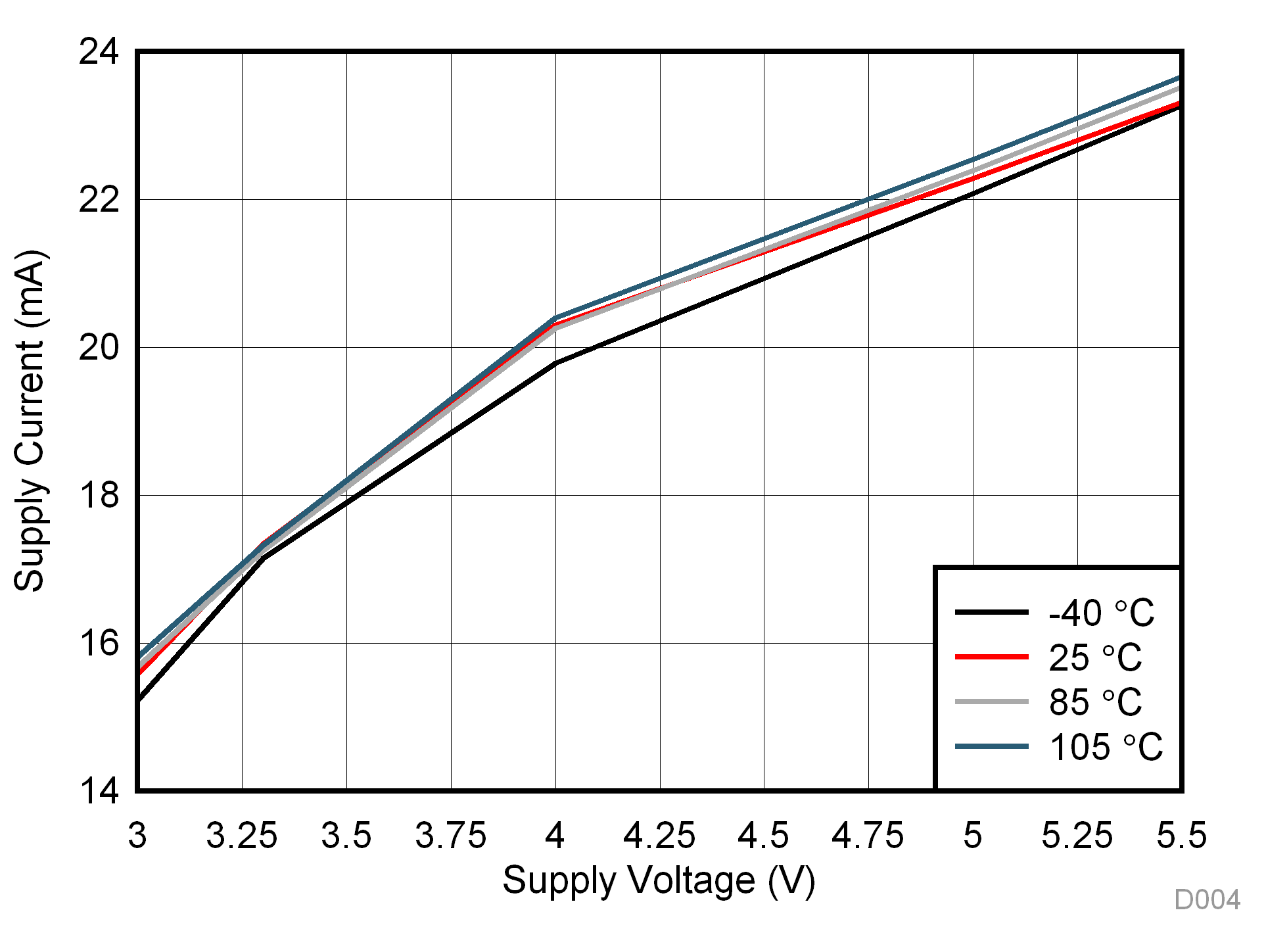
| REXT = 720 Ω | All Channels ON | |