SBVS129A May 2009 – July 2018 TLC5952
PRODUCTION DATA.
- 1 Features
- 2 Applications
- 3 Description
- 4 Revision History
- 5 Pin Configuration and Functions
- 6 Specifications
- 7 Parameter Measurement Information
- 8 Detailed Description
- 9 Power Supply Recommendations
- 10Device and Documentation Support
- 11Mechanical, Packaging, and Orderable Information
Package Options
Mechanical Data (Package|Pins)
- DAP|32
Thermal pad, mechanical data (Package|Pins)
- DAP|32
Orderable Information
8.4.2.2 Control-Data Latch
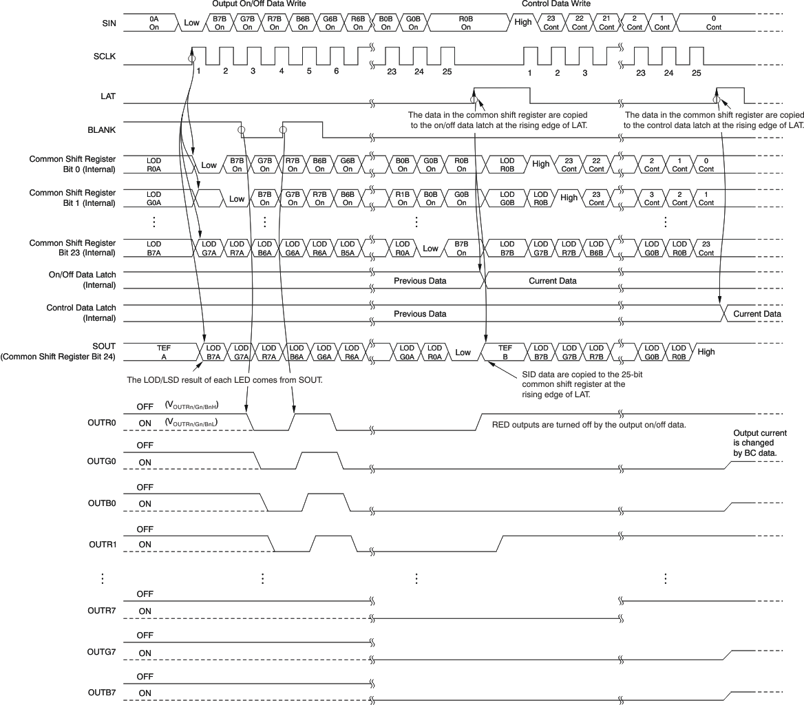
The control data latch is 24 bits long and is used to adjust the LED current for each color group (OUTR0-OUTR7, OUTG0-OUTG7, and OUTB0-OUTB7). The LED current for each group can be adjusted between 0% and 100% of IOLCMAX in 128 steps (7-bit resolution). This data latch is also used to select the error detection type, LED open detection (LOD) or LED short detection (LSD), and the threshold voltage. When the MSB of the common shift register is set to 1, the lower 24 bits are written to the control data latch on the rising edge of LAT. Table 4 shows the control data latch bit assignment.
When the device is powered on, the data in the control data latch are not set to a default value. Therefore, the control data latch data should be written to the latch before the constant-current outputs are turned on.
Table 4. Data Bit Assignment
| BITS | DESCRIPTION |
|---|---|
| 6–0 | Global brightness control data for RED group (OUTR0-OUTR7, data = 00h to 7Fh) |
| 13–7 | Global brightness control data for GREEN group (OUTG0-OUTG7, data = 00h to 7Fh) |
| 20–14 | Global brightness control data for BLUE group (OUTB0-OUTB7, data = 00h to 7Fh) |
| 23–21 | Detection voltage and type select (data = 0h to 7h)
0 = LED open detection with 0.3 V (typ) threshold 1 = LED open detection with 0.6 V (typ) threshold 2 = LED open detection with 0.9 V (typ) threshold 3 = LED open detection with 1.2 V (typ) threshold 4 = LED short detection with VCC × 60% (typ) threshold 5 = LED short detection with VCC × 70% (typ) threshold 6 = LED short detection with VCC × 80% (typ) threshold 7 = LED short detection with VCC × 90% (typ) threshold |
Figure 38 shows the operation to write data into the common shift register and control data latch.
 Figure 38. Data Write Operation