SBVS241 April 2014 TLC5954
PRODUCTION DATA.
- 1 Features
- 2 Applications
- 3 Description
- 4 Revision History
- 5 Pin Configuration and Functions
- 6 Specifications
- 7 Parameter Measurement Information
- 8 Detailed Description
- 9 Applications and Implementation
- 10Power Supply Recommendations
- 11Layout
- 12Device and Documentation Support
- 13Mechanical, Packaging, and Orderable Information
Package Options
Mechanical Data (Package|Pins)
- RTQ|56
Thermal pad, mechanical data (Package|Pins)
- RTQ|56
Orderable Information
6 Specifications
6.1 Absolute Maximum Ratings
over operating free-air temperature range (unless otherwise noted)(1)| MIN | MAX | UNIT | |||
|---|---|---|---|---|---|
| VCC | Supply voltage(2) | –0.3 | 4.0 | V | |
| VIN | Input voltage range | SIN, SCLK, LAT, BLANK | –0.3 | VCC + 0.3 | V |
| VOUT | Output voltage range | SOUT | –0.3 | VCC + 0.3 | V |
| OUTR0 to OUTR15, OUTG0 to OUTG15, OUTB0 to OUTB15 |
–0.3 | 11 | V | ||
| TJ (max) | Operating junction temperature | 150 | °C | ||
(1) Stresses beyond those listed under Absolute Maximum Ratings may cause permanent damage to the device. These are stress ratings only, and functional operation of the device at these or any other conditions beyond those indicated under Recommended Operating Conditions is not implied. Exposure to absolute-maximum-rated conditions for extended periods my affect device reliability.
(2) All voltages are with respect to device ground pin.
6.2 Handling Ratings
| MIN | MAX | UNIT | |||
|---|---|---|---|---|---|
| Tstg | Storage temperature range | –55 | 150 | °C | |
| V(ESD) | Electrostatic discharge | Human body model (HBM), per ANSI/ESDA/JEDEC JS-001, all pins(1) | –200 | 2000 | V |
| Charged device model (CDM), per JEDEC specification JESD22-C101, all pins(2) | –500 | 500 | V | ||
(1) JEDEC document JEP155 states that 500-V HBM allows safe manufacturing with a standard ESD control process.
(2) JEDEC document JEP157 states that 250-V CDM allows safe manufacturing with a standard ESD control process.
6.3 Recommended Operating Conditions
At TA= –40°C to +85°C, unless otherwise noted.| PARAMETER | TEST CONDITIONS | MIN | NOM | MAX | UNIT | |
|---|---|---|---|---|---|---|
| DC CHARACTERISTICS (VCC = 3 V to 3.6 V) | ||||||
| VCC | Supply voltage | 3.0 | 3.6 | V | ||
| VO | Voltage applied to output | OUTR0 to OUTR15, OUTG0 to OUTG15, OUTB0 to OUTB15 | 10 | V | ||
| VIH | High-level input voltage | SIN, SCLK, LAT, BLANK | 0.7 × VCC | VCC | V | |
| VIL | Low-level input voltage | SIN, SCLK, LAT, BLANK | GND | 0.3 × VCC | V | |
| IOH | High-level output current | SOUT | –2 | mA | ||
| IOL | Low-level output current | SOUT | 2 | mA | ||
| TA | Operating free-air temperature range | –40 | +85 | °C | ||
| TJ | Operating junction temperature range | –40 | +125 | °C | ||
| AC CHARACTERISTICS (VCC = 3 V to 3.6 V) | ||||||
| fCLK (SCLK) | Data shift clock frequency | SCLK | 30 | MHz | ||
| tWH0 | Pulse duration | SCLK | 10 | ns | ||
| tWL0 | SCLK | 10 | ns | |||
| tWH1 | LAT | 15 | ns | |||
| tWH2 | BLANK | 60 | ns | |||
| tWL2 | BLANK | 40 | ns | |||
| tSU0 | Setup time | SIN to SCLK↑ | 4 | ns | ||
| tSU1 | LAT↓ to SCLK↑ | 20 | ns | |||
| tSU2 | SCLK↑ resumes normal mode, BLANK↓, PSMODE bit = 01b | 12 | µs | |||
| tSU3 | LAT↑ for all data latching except all 0s resumes normal mode, BLANK↓, PSMODE bit = 10b | 12 | µs | |||
| tH0 | Hold time | SCLK↑ to SIN | 3 | ns | ||
| tH1 | SCLK↑ to LAT↑ | 10 | ns | |||
6.4 Thermal Information
| THERMAL METRIC(1) | TLC5954 | UNIT | |
|---|---|---|---|
| RTQ (VQFN) | |||
| 56 PINS | |||
| RθJA | Junction-to-ambient thermal resistance | 29.1 | °C/W |
| RθJCtop | Junction-to-case (top) thermal resistance | 16.3 | |
| RθJB | Junction-to-board thermal resistance | 7.7 | |
| ψJT | Junction-to-top characterization parameter | 0.3 | |
| ψJB | Junction-to-board characterization parameter | 7.7 | |
| RθJCbot | Junction-to-case (bottom) thermal resistance | 2.8 | |
(1) For more information about traditional and new thermal metrics, see the IC Package Thermal Metrics application report, SPRA953.
6.5 Electrical Characteristics
At TA = –40°C to +85°C and VCC = 3.0 V to 3.6 V, unless otherwise noted. Typical values are at TA = +25°C and VCC = 3.3 V.| PARAMETER | TEST CONDITIONS | MIN | TYP | MAX | UNIT | ||
|---|---|---|---|---|---|---|---|
| VOH | High-level output voltage | IOH = –2 mA at SOUT | VCC – 0.4 | VCC | V | ||
| VOL | Low-level output voltage | IOL = 2 mA at SOUT | 0.4 | V | |||
| VLOD0 | LED open-detection threshold | LODVLT = 000b | 0.15 | 0.20 | 0.25 | V | |
| VLOD1 | LODVLT = 001b, 101b, 110b, 111b | 0.25 | 0.30 | 0.35 | V | ||
| VLOD2 | LODVLT = 010b | 0.35 | 0.40 | 0.45 | V | ||
| VLOD3 | LODVLT = 011b | 0.45 | 0.50 | 0.55 | V | ||
| VLOD4 | LODVLT = 100b | 0.55 | 0.60 | 0.65 | V | ||
| VLSD0 | LED short-detection threshold | LSDVLT = 00b | 0.45 × VCC | 0.50 × VCC | 0.55 × VCC | V | |
| VLSD1 | LSDVLT = 01b | 0.65 × VCC | 0.70 × VCC | 0.75 × VCC | V | ||
| VLSD2 | LSDVLT = 10b, 11b | 0.85 × VCC | 0.90 × VCC | 0.95 × VCC | V | ||
| IIN | Input current | VIN = VCC or GND at SIN, SCLK, LAT, and BLANK | –1 | 1 | μA | ||
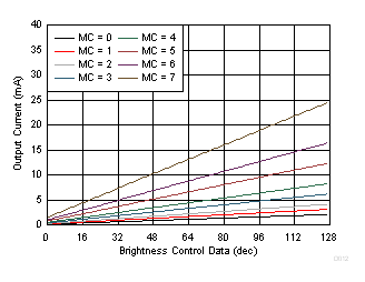
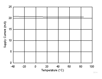
| ICC0 | Supply current (VCC) | SIN, SCLK, LAT = GND, BLANK = VCC, VOUTXn = 1 V, BCX = 7Fh, MC = 0h (IOUTRn, IOUTGn = 2.9-mA target, IOUTBn = 2.0-mA target)(5) | 15 | 19 | mA | ||
| ICC1 | SIN, SCLK, LAT = GND, BLANK = VCC, VOUTXn = 1 V, BCX = 7Fh, MC = 5h (IOUTRn, IOUTGn = 17.4-mA target, IOUTBn = 12.2-mA target) | 17.5 | 22 | mA | |||
| ICC2 | SIN, SCLK, LAT, BLANK = GND, all OUTXn = on, VOUTXn = 1 V, BCX = 7Fh, MC = 5h | 17.5 | 22 | mA | |||
| ICC3 | SIN, SCLK, LAT, BLANK = GND, all OUTXn = on, VOUTXn = 1 V, BCX = 7Fh, MC = 7h (IOUTRn, IOUTGn = 34.9-mA target, IOUTBn = 24.4-mA target) | 20.5 | 25.5 | mA | |||
| ICC4 | In power-save mode, SIN, SCLK, LAT = GND, BLANK = VCC |
7 | 60 | µA | |||
| IOLC0 | Constant output current | All OUTXn = on, VOUTXn = VOUTfix = 1 V, BC = 7Fh, MC = 7h, at OUTR0 to OUTR15 and OUTG0 to OUTG15 |
32.5 | 34.9 | 37.3 | mA | |
| IOLC1 | All OUTXn = on, VOUTXn = VOUTfix = 1 V, BC = 7Fh, MC = 7h, at OUTB0 to OUTB15 |
22.7 | 24.4 | 26.1 | mA | ||
| IOLKG | Output leakage current | BLANK = VCC, VOUTXn = VOUTfix = 10 V, MC = 7h, at OUTXn | TJ = +25°C | 0.1 | µA | ||
| TJ = +85°C | 0.2 | µA | |||||
| TJ = +125°C | 0.5 | µA | |||||
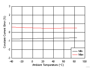
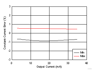
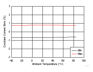
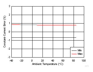
| ΔIOLC0 | Constant-current error (channel-to-channel)(1) |
All OUTXn = on, BCX = 7Fh, VOUTXn = VOUTfix = 1 V, MC = 7h, at same color group (OUTXn) | ±1% | ±3% | |||
| ΔIOLC1 | Constant-current error (device-to-device)(2) |
All OUTXn = on, BCX = 7Fh, VOUTXn = VOUTfix = 1 V, MC = 7h, at same color group (OUTXn) | ±0.5% | ±3% | |||
| ΔIOLC2 | Line regulation(3) | All OUTXn = on, BCX = 7Fh, VOUTXn = VOUTfix = 1 V, MC = 7h, at OUTXn | ±0.5 | ±1 | %/V | ||
| ΔIOLC3 | Load regulation(4) | All OUTXn = on, BCX = 7Fh, VOUTXn = 1 V to 3 V, VOUTfix = 1 V, MC = 7h, at OUTXn | ±1 | ±3 | %/V | ||
(1) The deviation of each output in the same color group (OUTRn, OUTGn, OUTBn) from the average of the same OUTXn group constant-current. Deviation is calculated by the formula:
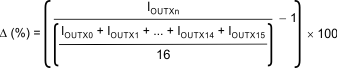
, where X = R, G, or B, and n = 0 to 15.
, where X = R, G, or B, and n = 0 to 15.
(2) The deviation of the OUTXn constant-current average from the ideal constant-current value. Deviation is calculated by the formula:
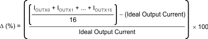
Ideal current is 34.9 mA for OUTRn and OUTGn. Ideal current is 24.4 mA for OUTBn with MC data equal to 7h.
, where X = R, G, or B, and n = 0 to 15.
Ideal current is 34.9 mA for OUTRn and OUTGn. Ideal current is 24.4 mA for OUTBn with MC data equal to 7h.
, where X = R, G, or B, and n = 0 to 15.
(3) Line regulation is calculated by the formula:
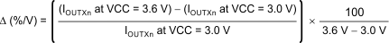
X = R, G, or B. n = 0 to 15.
X = R, G, or B. n = 0 to 15.
(4) Load regulation is calculated by the equation:
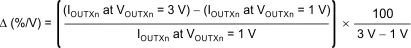
, where X = R, G, or B, and n = 0 to 15.
, where X = R, G, or B, and n = 0 to 15.
(5) X = R, G, and B. n = 0 to 15.
6.6 Switching Characteristics
At TA = –40°C to +85°C, VCC = 3.0 V to 3.6 V, CL = 15 pF, RL = 100 Ω for OUTRn and OUTGn, RL = 150 Ω for OUTBn,MC = 7h, and VLED = 4.5 V, unless otherwise noted. Typical values at TA = +25°C and VCC = 3.3 V.
| PARAMETER | TEST CONDITIONS | MIN | TYP | MAX | UNIT | |
|---|---|---|---|---|---|---|
| tR0 | Rise time | SOUT | 2 | 5 | ns | |
| tR1 | OUTXn, BCX = 7Fh(3) | 20 | 50 | ns | ||
| tF0 | Fall time | SOUT | 2 | 5 | ns | |
| tF1 | OUTXn, BCX = 7Fh | 20 | 50 | ns | ||
| tD0 | Propagation delay(1) | SCLK↑ to SOUT | 13 | 23 | ns | |
| tD1 | LAT↑ to OUTR0 on to off or OUTR0 off to on, BCX = 7Fh | 30 | 60 | ns | ||
| tD2 | BLANK↓↑ to OUTR0 on to off or OUTR0 off to on, BCX = 7Fh | 30 | 60 | ns | ||
| tD3 | OUTRn on to OUTGn on, OUTGn on to OUTBn on, and OUTBn on to the next OUTRn on, BCX = 7Fh | 1.5 | 5 | ns | ||
| tD4 | OUTRn off to OUTGn off, OUTGn off to OUTBn off, and OUTBn off to the next OUTRn off, BCX = 7Fh | 1.5 | 5 | ns | ||
| tD5 | LAT↑ to power-save mode by writing data for all OUTXn off | 150 | 300 | ns | ||
| tON_ERR | Output on-time error(2) | OUTXn on or off data = all 1s, BCX = 7Fh, 40-ns BLANK low-level one-shot pulse input | –35 | 35 | ns | |
(1) tD3 (OUTRn on to OUTGn on, OUTGn on to OUTBn on, and OUTBn on to the next OUTRn on) and tD4 (OUTRn off to OUTGn off, OUTGn off to OUTBn off, and OUTBn off to the next OUTRn off) are calculated by:
tD3 (ns) = (the propagation delay between OUTR0 on to OUTB7 on) / 47 and
tD4 (ns) = (the propagation delay between OUTR0 off to OUTB7 off) / 47.
tD3 (ns) = (the propagation delay between OUTR0 on to OUTB7 on) / 47 and
tD4 (ns) = (the propagation delay between OUTR0 off to OUTB7 off) / 47.
(2) Output on-time error (tON_ERR) is calculated by the formula: tON_ERR (ns) = tOUT_ON – BLANK low-level pulse duration.
tOUT_ON is the actual on-time of OUTXn.
tOUT_ON is the actual on-time of OUTXn.
(3) X = R, G, or B. n = 0 to 15.
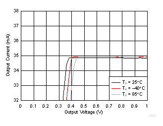
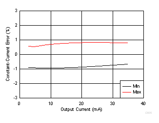
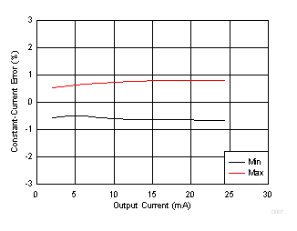
6.7 Typical Characteristics
At TA = +25°C and VCC = 3.3 V, unless otherwise noted.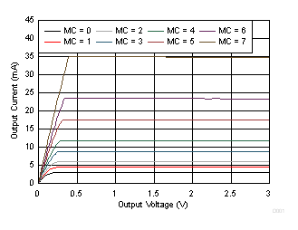
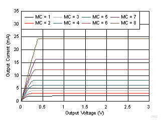
| BCR, BCG = 7Fh |
(OUTRn, OUTGn)
| BCR = BCG = 7Fh | MC = 7 |
(OUTRn, OUTGn)
| BCR = 7Fh | MC = 7 |
| BCB = 7Fh | MC = 7 |
| BCG = 7Fh | MC = 7h |
| BCR = BCG = 7Fh |
(OUTRn, OUTGn)
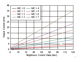
| SIN = 15 MHz | SCLK = 30 MHz | BCX = 7Fh |
| MC = 0h to 7h | All OUTXn = On | BLANK = Low |
| SOUT = No Load | VOUT = 0.8 V | |
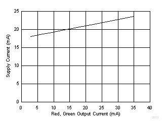
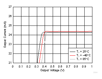
| VCC = 3.3 V | MC = 7h | BCX = 7Fh | VLED = 4.5 V | ||
| RL = 100 Ω (OUTRn, OUTGn) | RL = 150 Ω (OUTBn) | ||||
| CL = 15 pF | BLANK Low Pulse Duration = 40 ns | ||||
| BCB = 7Fh |
(OUTBn)
| BCB = 7Fh | MC = 7 |
(OUTBn)
| BCG = 7Fh | MC = 7 |
| BCR = 7Fh | MC = 7h |
| BCB = 7Fh | MC = 7 |
| BCB = 7Fh |
(OUTBn)
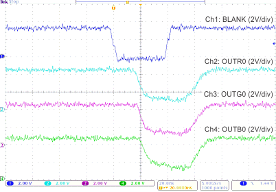
| SIN = 15 MHz | BCX = 7Fh | MC = 5h |
| All OUTXn = On | SCLK = 30 MHz | BLANK = Low |
| SOUT = No Load | VOUT = 0.8 V | |
| TA = –40°C to +85°C | ||