SLVSEB3A June   2018  – January 2019 TLC6946 , TLC6948

PRODUCTION DATA.  

  1. Features
  2. Applications
  3. Description
    1.     Device Images
      1.      Typical Application Schematic of TLC6948 With 48-Multiplexing
  4. Revision History
  5. Description (continued)
  6. Pin Configuration and Functions
    1.     Pin Functions
  7. Specifications
    1. 7.1 Absolute Maximum Ratings
    2. 7.2 ESD Ratings
    3. 7.3 Recommended Operating Conditions
    4. 7.4 Thermal Information
    5. 7.5 Electrical Characteristics
    6. 7.6 Switching Characteristics
    7. 7.7 Typical Characteristics
  8. Parameter Measurement Information
    1. 8.1 Pin Equivalent Input and Output Schematic Diagrams
  9. Detailed Description
    1. 9.1 Overview
    2. 9.2 Functional Block Diagram
    3. 9.3 Feature Description
      1. 9.3.1  Built-In 16Kb Display Memory (SRAM)
      2. 9.3.2  GCLK Dual-Edge Operation
      3. 9.3.3  Programmable Constant-Sink Channel Current
        1. 9.3.3.1 Global Brightness Control (BC)
        2. 9.3.3.2 Select RIREF for a Given BC
      4. 9.3.4  Grayscale (GS) Function (PWM Control)
      5. 9.3.5  Serial Data Interface
      6. 9.3.6  LED-Open Detection (LOD)
      7. 9.3.7  Caterpillar Removal
      8. 9.3.8  Precharge FET
      9. 9.3.9  Thermal Shutdown
      10. 9.3.10 IREF Resistor Short Protection (ISP)
    4. 9.4 Device Functional Modes
      1. 9.4.1 Normal Operating Mode
      2. 9.4.2 Power-Save Mode (PSM)
  10. 10Application and Implementation
    1. 10.1 Application Information
    2. 10.2 Typical Application
      1. 10.2.1 Design Requirements
      2. 10.2.2 Detailed Design Procedures
        1. 10.2.2.1 Power Supply Voltage
        2. 10.2.2.2 Channel Current and Brightness Control
        3. 10.2.2.3 SCLK and GCLK Frequency
      3. 10.2.3 Application Curves
  11. 11Power Supply Recommendations
  12. 12Layout
    1. 12.1 Layout Guidelines
    2. 12.2 Layout Examples
  13. 13Device and Documentation Support
    1. 13.1 Documentation Support
      1. 13.1.1 Related Documentation
    2. 13.2 Related Links
    3. 13.3 Receiving Notification of Documentation Updates
    4. 13.4 Community Resources
    5. 13.5 Trademarks
    6. 13.6 Electrostatic Discharge Caution
    7. 13.7 Glossary
  14. 14Mechanical, Packaging, and Orderable Information

Package Options

Mechanical Data (Package|Pins)
Thermal pad, mechanical data (Package|Pins)
Orderable Information

Typical Characteristics

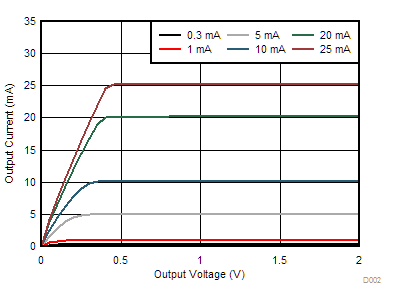
TLC6946 TLC6948 D002_SLVSEB3.gif
VCC = 5 V
Figure 2. Channel Sink Current vs OUTn Voltage
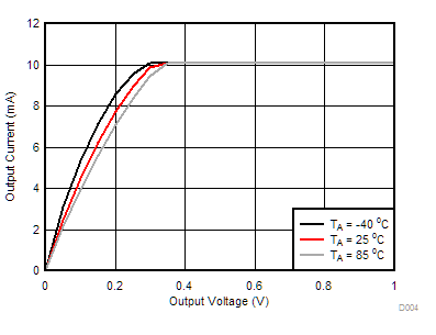
TLC6946 TLC6948 D004_SLVSEB3.gif
VCC = 5 V Temperature changing
Figure 4. Channel Sink Current vs OUTn Voltage
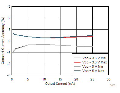
TLC6946 TLC6948 D005_SLVSEB3.gif
VOUTn = 1 V
Figure 6. Channel to Channel Accuracy vs OUTn Current
TLC6946 TLC6948 D008_SLVSEB3.gif
VCC = 5 V VOUTn = 1 V
Figure 8. Channel Sink Current vs Brightness Control (BC)
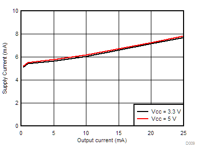
TLC6946 TLC6948 D009_SLVSEB3.gif
VOUTn = 1 V GCLK = 33 MHz GSn = FFFFh
Figure 10. Supply Current (ICC) vs Channel Sink Current
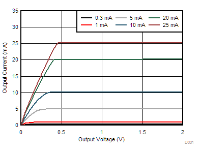
TLC6946 TLC6948 D001_SLVSEB3.gif
VCC = 3.3 V
Figure 3. Channel Sink Current vs OUTn Voltage
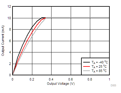
TLC6946 TLC6948 D003_SLVSEB3.gif
VCC = 3.3 V Temperature changing
Figure 5. Channel Sink Current vs OUTn Current
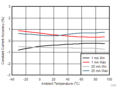
TLC6946 TLC6948 D006_SLVSEB3.gif
VOUTn = 1 V
Figure 7. Channel to Channel Accuracy vs Temperature
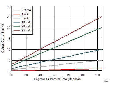
TLC6946 TLC6948 D007_SLVSEB3.gif
VCC = 3.3 V VOUTn = 1 V
Figure 9. Channel Sink Current vs Brightness Control (BC)
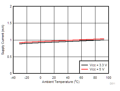
TLC6946 TLC6948 D011_SLVSEB3.gif
VOUTn = 1 V GCLK = 33 MHz GSn = 0000h
BC = 36h RIREF = 1.27 kΩ (10-mA target)
Figure 11. Supply Current (ICC) in Power-Save Mode vs Temperature