SBVS283F August   2016  – October 2020 TLV733P-Q1

PRODUCTION DATA  

  1. Features
  2. Applications
  3. Description
  4. Revision History
  5. Pin Configuration and Functions
  6. Specifications
    1. 6.1 Absolute Maximum Ratings
    2. 6.2 ESD Ratings
    3. 6.3 Recommended Operating Conditions
    4. 6.4 Thermal Information
    5. 6.5 Electrical Characteristics
    6. 6.6 Timing Requirements
    7. 6.7 Typical Characteristics
  7. Detailed Description
    1. 7.1 Overview
    2. 7.2 Functional Block Diagram
    3. 7.3 Feature Description
      1. 7.3.1 Undervoltage Lockout (UVLO)
      2. 7.3.2 Shutdown and Output Enable
      3. 7.3.3 Internal Foldback Current Limit
      4. 7.3.4 Thermal Shutdown
    4. 7.4 Device Functional Modes
      1. 7.4.1 Normal Operation
      2. 7.4.2 Dropout Operation
      3. 7.4.3 Disabled
  8. Application and Implementation
    1. 8.1 Application Information
      1. 8.1.1 Input and Output Capacitor Selection
      2. 8.1.2 Dropout Voltage
    2. 8.2 Typical Applications
      1. 8.2.1 DC-DC Converter Post Regulation
        1. 8.2.1.1 Design Requirements
        2. 8.2.1.2 Design Considerations
        3. 8.2.1.3 Application Curve
      2. 8.2.2 Capacitor-Free Operation from a Battery Input Supply
        1. 8.2.2.1 Design Requirements
        2. 8.2.2.2 Design Considerations
        3. 8.2.2.3 Application Curve
  9. Layout
    1. 9.1 Layout Guidelines
    2. 9.2 Layout Examples
  10. 10Device and Documentation Support
    1. 10.1 Device Support
      1. 10.1.1 Development Support
        1. 10.1.1.1 Evaluation Module
      2. 10.1.2 Device Nomenclature
    2. 10.2 Receiving Notification of Documentation Updates
    3. 10.3 Support Resources
    4. 10.4 Trademarks
    5. 10.5 Electrostatic Discharge Caution
    6. 10.6 Glossary

Package Options

Mechanical Data (Package|Pins)
Thermal pad, mechanical data (Package|Pins)
Orderable Information

Shutdown and Output Enable

The enable pin (EN) is active high. Enable the device by forcing the EN pin to exceed VEN(HI). Turn off the device by forcing the EN pin to drop below VEN(LO). If shutdown capability is not required, connect EN to IN. There is no internal pulldown resistor connected to the EN pin.

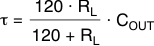
The TLV733P-Q1 has an internal pulldown MOSFET that connects a 120-Ω resistor to ground when the device is disabled. The discharge time after disabling depends on the output capacitance (COUT) and the load resistance (RL) in parallel with the 120-Ω pulldown resistor. The time constant is calculated in Equation 1:

Equation 1. GUID-97716BDC-193F-482A-AFCB-14775EC72443-low.gif