SBVS283F August 2016 – October 2020 TLV733P-Q1
PRODUCTION DATA
- 1 Features
- 2 Applications
- 3 Description
- 4 Revision History
- 5 Pin Configuration and Functions
- 6 Specifications
- 7 Detailed Description
- 8 Application and Implementation
- 9 Layout
- 10Device and Documentation Support
Package Options
Mechanical Data (Package|Pins)
Thermal pad, mechanical data (Package|Pins)
- DRV|6
Orderable Information
3 Description
The TLV733P-Q1 family of low dropout (LDO) linear regulators are ultra-small, low quiescent current LDOs that can source 300 mA with good line and load transient performance. These devices provide a typical accuracy of 1%.
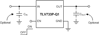
The TLV733P-Q1 family is designed with a modern capacitor-free architecture to ensure stability without an input or output capacitor. The removal of the output capacitor allows for a very small solution size, and can eliminate inrush current at startup. Furthermore, the TLV733P-Q1 family is also stable with ceramic output capacitors if an output capacitor is necessary. The TLV733P-Q1 family also provides foldback current control during device power-up and enabling if an output capacitor is used. This functionality is especially important in battery-operated devices.
The TLV733P-Q1 family provides an active pulldown circuit to quickly discharge output loads when disabled.
The TLV733P-Q1 family is available in the 6-pin DRV (WSON) and 5-pin DBV (SOT-23) packages.
| PART NUMBER | PACKAGE | BODY SIZE (NOM) |
|---|---|---|
| TLV733P-Q1 | WSON (6) | 2.00 mm × 2.00 mm |
| SOT-23 (5) | 2.90 mm × 1.60 mm |
 Typical Application Circuit
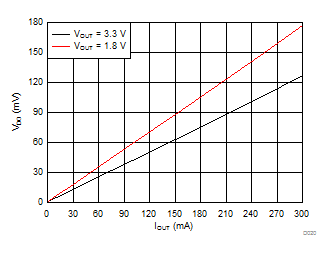
 Dropout Voltage vs Output Current