SBVS351D April 2018 – October 2023 TLV758P
PRODUCTION DATA
- 1
- 1 Features
- 2 Applications
- 3 Description
- 4 Pin Configuration and Functions
- 5 Specifications
- 6 Detailed Description
- 7 Application and Implementation
- 8 Device and Documentation Support
- 9 Revision History
- 10Mechanical, Packaging, and Orderable Information
Package Options
Mechanical Data (Package|Pins)
Thermal pad, mechanical data (Package|Pins)
- DRV|6
Orderable Information
7.2.2.1 Input Current
During normal operation, the input current to the LDO is approximately equal to the output current of the LDO. During start-up, the input current is higher as a result of the inrush current charging the output capacitor. Use Equation 6 to calculate the current through the input.
Equation 6. 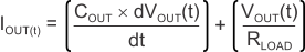
where:
- VOUT(t) is the instantaneous output voltage of the turn-on ramp
- dVOUT(t) / dt is the slope of the VOUT ramp
- RLOAD is the resistive load impedance