SBOS685C April 2014 – July 2015 TMP007
PRODUCTION DATA.
- 1 Features
- 2 Applications
- 3 Description
- 4 Revision History
- 5 Pin Configuration and Functions
- 6 Specifications
-
7 Detailed Description
- 7.1 Overview
- 7.2 Functional Block Diagram
- 7.3
Feature Description
- 7.3.1 Spectral Responsivity
- 7.3.2 Field of View and Angular Response
- 7.3.3 Thermopile Principles and Operation
- 7.3.4 Object Temperature Calculation
- 7.3.5 Calibration
- 7.3.6 Sensor Voltage Format
- 7.3.7 Temperature Format
- 7.3.8 Serial Interface
- 7.4 Device Functional Modes
- 7.5
Register Maps
- 7.5.1 Sensor Voltage Result Register (address = 00h) [reset = 0000h]
- 7.5.2 TDIE Local Temperature Result Register (address = 01h) [reset = 0000h]
- 7.5.3 Configuration Register (address = 02h) [reset = 1440h]
- 7.5.4 TOBJ Object Temperature Result Register (address = 03h) [reset = 0000h]
- 7.5.5 Status Register (address = 04h) [reset = 0000h]
- 7.5.6 Status Mask and Enable Register (address = 05h) [reset = 0000h]
- 7.5.7 TOBJ Object Temperature High-Limit Register (address = 06h) [reset = 7FC0h]
- 7.5.8 TOBJ Object Temperature Low-Limit Register (address = 07h) [reset = 8000h]
- 7.5.9 TDIE Local Temperature High-Limit Register (address = 08h) [reset = 7FC0h]
- 7.5.10 TDIE Local Temperature Low-Limit Register (address = 09h) [reset = 8000h]
- 7.5.11
Coefficient Registers
- 7.5.11.1 S0 Coefficient Register (address = 0Ah) [reset = 260Eh]
- 7.5.11.2 A1 Coefficient Register (address = 0Bh) [reset = 0106h]
- 7.5.11.3 A2 Coefficient Register (address = 0Ch) [reset = FF9Bh]
- 7.5.11.4 B0 Coefficient Register (address = 0Dh) [reset = FF3Ah]
- 7.5.11.5 B1 Coefficient Register (address = 0Eh) [reset = FF71h]
- 7.5.11.6 B2 Coefficient Register (address = 0Fh) [reset = 0553h]
- 7.5.11.7 C2 Coefficient Register (address = 10h) [reset = 0000h]
- 7.5.11.8 TC0 Coefficient Register (address = 11h) [reset = 0034h]
- 7.5.11.9 TC1 Coefficient Register (address = 12h) [reset = 0000h]
- 7.5.12 Manufacturer ID Register (address = 1Eh) [reset = 5449h]
- 7.5.13 Device ID Register (address = 1Fh) [reset = 0078h]
- 7.5.14 Memory Access Register (address = 2Ah) [reset = 0000h]
- 8 Application and Implementation
- 9 Power-Supply Recommendations
- 10Layout
- 11Device and Documentation Support
- 12Mechanical, Packaging, and Orderable Information
Package Options
Mechanical Data (Package|Pins)
- YZF|8
Thermal pad, mechanical data (Package|Pins)
Orderable Information
5 Pin Configuration and Functions
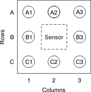
YZF Package
8-Pin DSBGA
Top View

Pin Functions
| PIN | DESCRIPTION | |
|---|---|---|
| NAME | NO. | |
| ADR0 | C1 | Input address 0 selection pin |
| ADR1 | B1 | Input address 1 selection pin |
| AGND | A2 | Analog ground |
| ALERT | C2 | Alert output pin; active low, open-drain. Requires a pull-up resistor to (1.6 V to 5.5 V) supply |
| DGND | A1 | Digital ground |
| SCL | B3 | Input clock pin |
| SDA | C3 | Input/output data pin; open-drain; requires pull-up resistor to (1.6 V to 5.5 V) supply |
| V+ | A3 | Supply voltage (2.5 V to 5.5 V) |