SBOS473J March   2009  – February 2024 TMP112

PRODUCTION DATA  

  1.   1
  2. Features
  3. Applications
  4. Description
  5. Device Comparison
  6. Pin Configuration and Functions
  7. Specifications
    1. 6.1 Absolute Maximum Ratings
    2. 6.2 Handling Ratings
    3. 6.3 Recommended Operating Conditions
    4. 6.4 Thermal Information
    5. 6.5 Electrical Characteristics
    6. 6.6 Timing Requirements
    7. 6.7 Timing Diagrams
    8. 6.8 Typical Characteristics (TMP112A/B/N)
    9. 6.9 Typical Characteristics (TMP112Dx)
  8. Detailed Description
    1. 7.1 Overview
    2. 7.2 Functional Block Diagrams
    3. 7.3 Feature Description
      1. 7.3.1 Digital Temperature Output
      2. 7.3.2 Serial Interface
        1. 7.3.2.1 Bus Overview
        2. 7.3.2.2 Serial Bus Address
        3. 7.3.2.3 Writing and Reading Operation
        4. 7.3.2.4 Slave Mode Operations
          1. 7.3.2.4.1 Slave Receiver Mode
          2. 7.3.2.4.2 Slave Transmitter Mode
        5. 7.3.2.5 SMBus Alert Function
        6. 7.3.2.6 General Call
        7. 7.3.2.7 High-Speed (Hs) Mode
        8. 7.3.2.8 Timeout Function
        9. 7.3.2.9 Timing Diagrams
          1. 7.3.2.9.1 Two-Wire Timing Diagrams
    4. 7.4 Device Functional Modes
      1. 7.4.1 Continuous-Conversion Mode
      2. 7.4.2 Extended Mode (EM)
      3. 7.4.3 One-Shot/Conversion Ready Mode (OS)
      4. 7.4.4 Thermostat Mode (TM)
        1. 7.4.4.1 Comparator Mode (TM = 0)
        2. 7.4.4.2 Interrupt Mode (TM = 1)
    5. 7.5 Programming
      1. 7.5.1 Pointer Register
      2. 7.5.2 Temperature Register
      3. 7.5.3 Configuration Register
        1. 7.5.3.1 Shutdown Mode (SD)
        2. 7.5.3.2 Thermostat Mode (TM)
        3. 7.5.3.3 Polarity (POL)
        4. 7.5.3.4 Fault Queue (F1/F0)
        5. 7.5.3.5 Converter Resolution (R1 and R0)
        6. 7.5.3.6 One-Shot (OS)
        7. 7.5.3.7 Extended Mode (EM)
        8. 7.5.3.8 Alert (AL)
      4. 7.5.4 High- and Low-Limit Register
  9. Application and Implementation
    1. 8.1 Application Information
    2. 8.2 Typical Application
      1. 8.2.1 Design Requirements
      2. 8.2.2 Detailed Design Procedure
      3. 8.2.3 Application Curves
      4. 8.2.4 Power Supply Recommendations
    3. 8.3 Layout
      1. 8.3.1 Layout Guidelines
      2. 8.3.2 Layout Example
  10. Device and Documentation Support
    1. 9.1 Documentation Support
      1. 9.1.1 Related Documentation
    2. 9.2 Receiving Notification of Documentation Updates
    3. 9.3 Support Resources
    4. 9.4 Trademarks
    5. 9.5 Electrostatic Discharge Caution
    6. 9.6 Glossary
  11. 10Revision History
  12. 11Mechanical, Packaging, and Orderable Information

Package Options

Mechanical Data (Package|Pins)
Thermal pad, mechanical data (Package|Pins)
Orderable Information

Pin Configuration and Functions

DPW Package
5-Pin X2SON
TMP112D
(Top View)
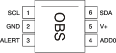
GUID-25E48344-B173-45DF-8E4F-51A8F8CB7C71-low.gifDRL Package
6-Pin SOT563
(Top View)
DPW Package
5-Pin X2SON
TMP112D0/D1/D2/D3
(Top View)
Table 5-1 Pin Function
PIN Type(1) DESCRIPTION
NAME NO. TMP112A/B/N NO. TMP112D NO. TMP112D0/1/2/3
SCL 1 2 2 I Serial clock
GND 2 1 1 Ground
Pin-1 has curved edges in TMP112Dx.
ALERT 3 - 3 O Overtemperature alert. Open-drain output; requires a pullup resistor.
Note: Connecting to GND if Alert pin is not used is preferred.
ADD0 4 3 - I Address Select. Connect to V+, GND, SDA or SCL
V+ 5 5 5 I Supply voltage, 1.4 V to 3.6 V
SDA 6 4 4 I/O Serial data. Open-drain output; requires a pullup resistor.
I = Input; O = Output, I/O = Input or Output