SBOS740A May   2017  – May 2019 TMP116

PRODUCTION DATA.  

  1. Features
  2. Applications
  3. Description
    1.     Device Images
      1.      Simplified Schematic
      2.      Temperature Accuracy
  4. Revision History
  5. Pin Configuration and Functions
    1.     Pin Functions
  6. Specifications
    1. 6.1 Absolute Maximum Ratings
    2. 6.2 ESD Ratings
    3. 6.3 Recommended Operating Conditions
    4. 6.4 Thermal Information
    5. 6.5 Electrical Characteristics
    6. 6.6 Two-Wire Interface Timing
    7. 6.7 Typical Characteristics
  7. Detailed Description
    1. 7.1 Overview
    2. 7.2 Functional Block Diagrams
    3. 7.3 Feature Description
      1. 7.3.1 Power Up
      2. 7.3.2 Temperature Result and Limits
    4. 7.4 Device Functional Modes
      1. 7.4.1 Temperature Conversions
        1. 7.4.1.1 Conversion Cycle
        2. 7.4.1.2 Averaging
        3. 7.4.1.3 Continuous Conversion Mode (CC)
        4. 7.4.1.4 Shutdown Mode (SD)
        5. 7.4.1.5 One-Shot Mode (OS)
      2. 7.4.2 Therm and Alert Modes
        1. 7.4.2.1 Alert Mode
        2. 7.4.2.2 Therm Mode
    5. 7.5 Programming
      1. 7.5.1 EEPROM Programming
        1. 7.5.1.1 EEPROM Overview
        2. 7.5.1.2 Programming the EEPROM
      2. 7.5.2 Pointer Register
      3. 7.5.3 I2C and SMBus Interface
        1. 7.5.3.1 Serial Interface
          1. 7.5.3.1.1 Bus Overview
          2. 7.5.3.1.2 Serial Bus Address
          3. 7.5.3.1.3 Writing and Reading Operation
          4. 7.5.3.1.4 Slave Mode Operations
            1. 7.5.3.1.4.1 Slave Receiver Mode
            2. 7.5.3.1.4.2 Slave Transmitter Mode
          5. 7.5.3.1.5 SMBus Alert Function
          6. 7.5.3.1.6 General-Call Reset Function
          7. 7.5.3.1.7 Timeout Function
          8. 7.5.3.1.8 Timing Diagrams
    6. 7.6 Registers Map
      1. 7.6.1 Register Descriptions
        1. 7.6.1.1  Temperature Register (address = 00h) [default reset = 8000h]
          1. Table 5. Temperature Register Field Descriptions
        2. 7.6.1.2  Configuration Register (address = 01h) [Factory default reset = 0220h]
          1. Table 6. Configuration Register Field Descriptions
        3. 7.6.1.3  High Limit Register (address = 02h) [Factory default reset = 6000h]
          1. Table 8. High Limit Register Field Descriptions
        4. 7.6.1.4  Low Limit Register (address = 03h) [Factory default reset = 8000h]
          1. Table 9. Low Limit Register Field Descriptions
        5. 7.6.1.5  EEPROM Unlock Register (address = 04h) [reset = 0000h]
          1. Table 10. EEPROM Unlock Register Field Descriptions
        6. 7.6.1.6  EEPROM1 Register (address = 05h) [reset = XXXXh]
          1. Table 11. EEPROM1 Register Field Descriptions
        7. 7.6.1.7  EEPROM2 Register (address = 06h) [reset = XXXXh]
          1. Table 12. EEPROM2 Register Field Descriptions
        8. 7.6.1.8  EEPROM3 Register (address = 07h) [reset = 0000h]
          1. Table 13. EEPROM3 Register Field Descriptions
        9. 7.6.1.9  EEPROM4 Register (address = 08h) [reset = XXXXh]
          1. Table 14. EEPROM4 Register Field Descriptions
        10. 7.6.1.10 Device ID Register (address = 0Fh) [reset = 1116h]
          1. Table 15. Device ID Register Field Descriptions
  8. Application and Implementation
    1. 8.1 Application Information
      1. 8.1.1 Typical Application
        1. 8.1.1.1 Design Requirements
        2. 8.1.1.2 Detailed Design Procedure
          1. 8.1.1.2.1 Noise and Averaging
          2. 8.1.1.2.2 Self-Heating Effect (SHE)
          3. 8.1.1.2.3 Synchronized Temperature Measurements
  9. Power Supply Recommendations
  10. 10Layout
    1. 10.1 Layout Guidelines
    2. 10.2 Layout Example
  11. 11Device and Documentation Support
    1. 11.1 Documentation Support
      1. 11.1.1 Related Documentation
    2. 11.2 Receiving Notification of Documentation Updates
    3. 11.3 Community Resources
    4. 11.4 Trademarks
    5. 11.5 Electrostatic Discharge Caution
    6. 11.6 Glossary
  12. 12Mechanical, Packaging, and Orderable Information

Package Options

Refer to the PDF data sheet for device specific package drawings

Mechanical Data (Package|Pins)
  • DRV|6
Thermal pad, mechanical data (Package|Pins)
Orderable Information

Conversion Cycle

When the device is operating in continuous conversion mode (see the Continuous Conversion Mode (CC) section), every conversion cycle consists of an active conversion period followed by a standby period. During active conversion the device typically consumes 135 µA, and during the low-power standby period the device typically consumes 1.25 µA, as indicated in Table 1. Figure 19 shows a current consumption profile of a conversion cycle. The duration of the active conversion period and standby period can be configured using the CONV[2:0] and AVG[1:0] bits in the configuration register, thereby allowing the average current consumption of the device to be optimized based on the application requirements. Changing the conversion cycle period also affects the temperature result update rate because the temperature result register is updated at the end of every conversion or averaging cycle.
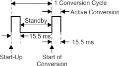
TMP116 TMP116N ai_conv_sbos740.gifFigure 19. Conversion Cycle Timing Diagram