SBOS740A May   2017  – May 2019 TMP116

PRODUCTION DATA.  

  1. Features
  2. Applications
  3. Description
    1.     Device Images
      1.      Simplified Schematic
      2.      Temperature Accuracy
  4. Revision History
  5. Pin Configuration and Functions
    1.     Pin Functions
  6. Specifications
    1. 6.1 Absolute Maximum Ratings
    2. 6.2 ESD Ratings
    3. 6.3 Recommended Operating Conditions
    4. 6.4 Thermal Information
    5. 6.5 Electrical Characteristics
    6. 6.6 Two-Wire Interface Timing
    7. 6.7 Typical Characteristics
  7. Detailed Description
    1. 7.1 Overview
    2. 7.2 Functional Block Diagrams
    3. 7.3 Feature Description
      1. 7.3.1 Power Up
      2. 7.3.2 Temperature Result and Limits
    4. 7.4 Device Functional Modes
      1. 7.4.1 Temperature Conversions
        1. 7.4.1.1 Conversion Cycle
        2. 7.4.1.2 Averaging
        3. 7.4.1.3 Continuous Conversion Mode (CC)
        4. 7.4.1.4 Shutdown Mode (SD)
        5. 7.4.1.5 One-Shot Mode (OS)
      2. 7.4.2 Therm and Alert Modes
        1. 7.4.2.1 Alert Mode
        2. 7.4.2.2 Therm Mode
    5. 7.5 Programming
      1. 7.5.1 EEPROM Programming
        1. 7.5.1.1 EEPROM Overview
        2. 7.5.1.2 Programming the EEPROM
      2. 7.5.2 Pointer Register
      3. 7.5.3 I2C and SMBus Interface
        1. 7.5.3.1 Serial Interface
          1. 7.5.3.1.1 Bus Overview
          2. 7.5.3.1.2 Serial Bus Address
          3. 7.5.3.1.3 Writing and Reading Operation
          4. 7.5.3.1.4 Slave Mode Operations
            1. 7.5.3.1.4.1 Slave Receiver Mode
            2. 7.5.3.1.4.2 Slave Transmitter Mode
          5. 7.5.3.1.5 SMBus Alert Function
          6. 7.5.3.1.6 General-Call Reset Function
          7. 7.5.3.1.7 Timeout Function
          8. 7.5.3.1.8 Timing Diagrams
    6. 7.6 Registers Map
      1. 7.6.1 Register Descriptions
        1. 7.6.1.1  Temperature Register (address = 00h) [default reset = 8000h]
          1. Table 5. Temperature Register Field Descriptions
        2. 7.6.1.2  Configuration Register (address = 01h) [Factory default reset = 0220h]
          1. Table 6. Configuration Register Field Descriptions
        3. 7.6.1.3  High Limit Register (address = 02h) [Factory default reset = 6000h]
          1. Table 8. High Limit Register Field Descriptions
        4. 7.6.1.4  Low Limit Register (address = 03h) [Factory default reset = 8000h]
          1. Table 9. Low Limit Register Field Descriptions
        5. 7.6.1.5  EEPROM Unlock Register (address = 04h) [reset = 0000h]
          1. Table 10. EEPROM Unlock Register Field Descriptions
        6. 7.6.1.6  EEPROM1 Register (address = 05h) [reset = XXXXh]
          1. Table 11. EEPROM1 Register Field Descriptions
        7. 7.6.1.7  EEPROM2 Register (address = 06h) [reset = XXXXh]
          1. Table 12. EEPROM2 Register Field Descriptions
        8. 7.6.1.8  EEPROM3 Register (address = 07h) [reset = 0000h]
          1. Table 13. EEPROM3 Register Field Descriptions
        9. 7.6.1.9  EEPROM4 Register (address = 08h) [reset = XXXXh]
          1. Table 14. EEPROM4 Register Field Descriptions
        10. 7.6.1.10 Device ID Register (address = 0Fh) [reset = 1116h]
          1. Table 15. Device ID Register Field Descriptions
  8. Application and Implementation
    1. 8.1 Application Information
      1. 8.1.1 Typical Application
        1. 8.1.1.1 Design Requirements
        2. 8.1.1.2 Detailed Design Procedure
          1. 8.1.1.2.1 Noise and Averaging
          2. 8.1.1.2.2 Self-Heating Effect (SHE)
          3. 8.1.1.2.3 Synchronized Temperature Measurements
  9. Power Supply Recommendations
  10. 10Layout
    1. 10.1 Layout Guidelines
    2. 10.2 Layout Example
  11. 11Device and Documentation Support
    1. 11.1 Documentation Support
      1. 11.1.1 Related Documentation
    2. 11.2 Receiving Notification of Documentation Updates
    3. 11.3 Community Resources
    4. 11.4 Trademarks
    5. 11.5 Electrostatic Discharge Caution
    6. 11.6 Glossary
  12. 12Mechanical, Packaging, and Orderable Information

Package Options

Refer to the PDF data sheet for device specific package drawings

Mechanical Data (Package|Pins)
  • DRV|6
Thermal pad, mechanical data (Package|Pins)
Orderable Information

Typical Characteristics

at TA = 25°C, V+ = 3.3 V, and measurement taken in oil bath (unless otherwise noted)
TMP116 TMP116N D024_SBOS740.gif
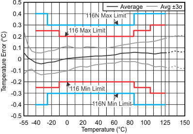
1-Hz conversion cycle, 8 averages mode
Figure 2. Temperature Error vs Temperature
TMP116 TMP116N D002_SBOS740.gif
Continuous conversion, no conversion cycle normalized to 3.3V
Figure 4. Temperature Error vs Supply Voltage in still air
TMP116 TMP116N D004_SBOS740.gif
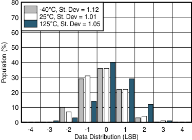
Figure 6. Data Reading Distribution Over Temperature
(No Averaging)
TMP116 TMP116N C001_SBOS740.gif
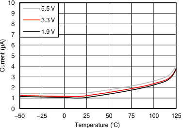
Serial bus inactive
Figure 8. Quiescent Current in Shutdown Mode
TMP116 TMP116N D007_SBOS740.gif
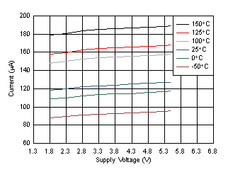
Continuous conversion mode, serial bus inactive
Figure 10. Quiescent Current During Active Conversion
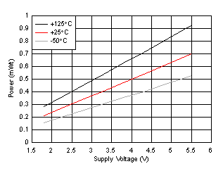
TMP116 TMP116N D016_SBOS740.gif
Serial bus inactive
Figure 12. Power Consumption During Active Conversion
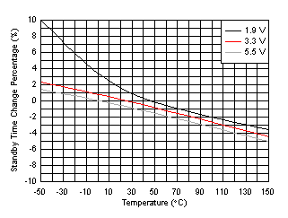
TMP116 TMP116N D026_SBOS740.gif
Normalized to 25°C and V+ = 3.3 V
Figure 14. Standby Time vs Temperature
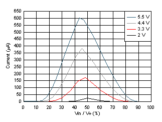
TMP116 TMP116N D021_SBOS740.gif
Input voltage of SCL, SDA, or ADD0 pin
Figure 16. Supply Current vs Input Cell Input Voltage
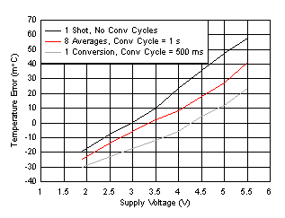
TMP116 TMP116N D001_SBOS740.gif
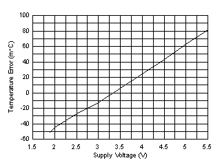
Figure 3. Temperature Error vs Supply Voltage
TMP116 TMP116N D003_SBOS740.gif
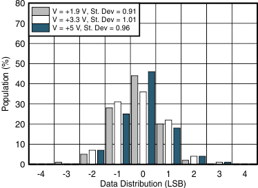
Figure 5. Data Reading Distribution Over Supply Voltage
(No Averaging)
TMP116 TMP116N D005_SBOS740.gif
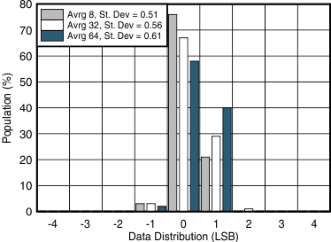
Figure 7. Data Reading Distribution Over Averaging Number
TMP116 TMP116N C002_SBOS740.gif
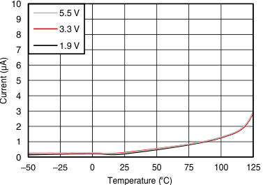
Serial bus inactive
Figure 9. Quiescent Current in Standby Mode
TMP116 TMP116N D010_SBOS740.gif
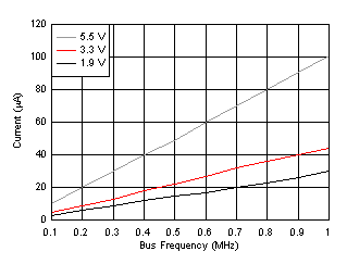
SCL, SDA, ADD0 pins are constantly clocked
Figure 11. Quiescent Current in Shutdown Mode
TMP116 TMP116N D023_SBOS740.gif
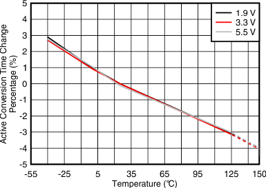
Normalized to 25°C and V+ = 3.3 V
Figure 13. Active Conversion Time vs Temperature
TMP116 TMP116N D022_SBOS740.gif
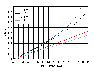
Figure 15. ALERT Pin Output Voltage vs Pin Sink Current