SBOS466B December 2009 – December 2018 TMP20
PRODUCTION DATA.
- 1 Features
- 2 Applications
- 3 Description
- 4 Revision History
- 5 Pin Configuration and Functions
- 6 Specifications
- 7 Detailed Description
- 8 Application and Implementation
- 9 Power Supply Recommendations
- 10Layout
- 11Device and Documentation Support
- 12Mechanical, Packaging, and Orderable Information
Package Options
Mechanical Data (Package|Pins)
Thermal pad, mechanical data (Package|Pins)
Orderable Information
8.1.1 Output Drive and Capacitive Loads
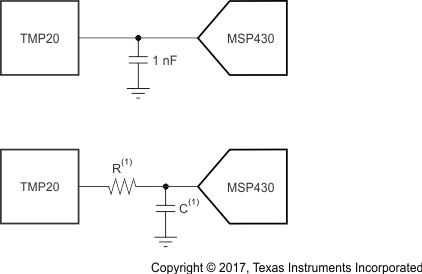
When used in noisy environments, adding a capacitor from the output to ground with a series resistor filters the TMP20 output; this configuration is shown in Figure 11. The TMP20 can drive up to 1 nF of load capacitance while sourcing and sinking 600 μA. Under this condition, capacitive loads in the range of 1 nF to 10 μF require a 150-Ω series output resistor to achieve a stable temperature measurement. The output impedance of the TMP20 is typically 10 Ω when sinking currents and less than 1 Ω when sourcing current, as shown in Figure 1.

1.
Figure 11. TMP20 Output Filtering NOINDENT:
A series resistor (R) may be required depending upon the amount of capacitance (C) and the amount of source and sink current drawn from the output of the TMP20.