SBOS486I July 2009 – December 2018 TMP303
PRODUCTION DATA.
- 1 Features
- 2 Applications
- 3 Description
- 4 Revision History
- 5 Device Options
- 6 Pin Configuration and Functions
- 7 Specifications
- 8 Detailed Description
- 9 Application and Implementation
- 10Power Supply Recommendations
- 11Layout
- 12Device and Documentation Support
- 13Mechanical, Packaging, and Orderable Information
Package Options
Mechanical Data (Package|Pins)
- DRL|6
Thermal pad, mechanical data (Package|Pins)
Orderable Information
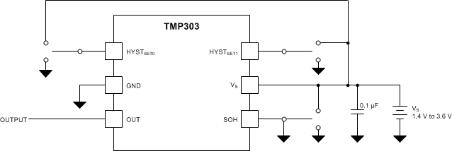
9.2.2 TMP303 With Switches
Figure 16 shows the most generic implementation of the TMP303 family of devices. Switches are shown connecting the HYSTSET0 and HYSTSET1 pins to either VS or GND. The use of switches is not a requirement; the switches are shown only to illustrate the various pin connection combinations. In practice, connecting the HYSTSET0 and HYSTSET1 pins to ground or directly to the VS pin is sufficient and minimizes board space and cost. If additional flexibility is desired, connections from the HYSTSET0 and HYSTSET1 pins can be made through 0-Ω resistors, which can be either populated or not, depending upon the desired connection.
 Figure 16. TMP303 With Switches